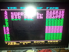
This evening I had a few minutes to implement the next IPC improvement I had in mind. This one is just implementing the simple end of instruction pipeline for instructions where it is possible, the same as I have already done for single byte instructions, and the same as what the real 6502 has always done.
The result is a nice little speed up as the pictures show.
This is among the last of the speed ups that I will do before a substantial reimplementation of the CPU to make it table driven. Using a table reduces the FPGA logic consumption a lot, and also has the potential to allow the CPU speed to be increased quite a bit, hopefully to 64MHz or even 96MHz all going well. But it is really the logic reduction that matters, so that I have space to implement the missing features in the C65GS.


Hey Paul, enjoying your progress. Any thoughts as to how you might handle SID? Would be nice to use original to maintain compatibility?
ReplyDeleteHowdy Simon,
DeleteI am planning to make a daughter board with room for 2 SIDs. I may also add an emulation option at some point.
Paul.
It will be nice but consider to use SwinSid instead of the original SID, justo to avoid depletion of chips that could be used to repair real C64/128.
ReplyDeletePS: congratulations for the excellent work!
Hello,
DeleteI expect I will have SID sockets, so something like the swinsid could be used once it is finished enough.
As for depleting the stocks of real SIDs, I have found a University fab that could in theory make new SID chips. But we need to first help visual-6502 project fully reverse engineer the SID and work out layer thicknesses etc to be able to do this.
Paul.
Im a total noob with this stuff Paul, but couldnt you improve performance by implementing multi-byte pseudo-ops? eg, SEC SBC, CLC ADC.... opcodes that are commonly seen together, treat as a single op?
ReplyDeleteLike I said, Im a noob :)
Hi Simon,
ReplyDeleteYou are quite right, it's called "super-scalar" meaning more than one instruction at a time, and is a common method on modern CPUs. However, this requires that you can fetch memory faster than you can execute. On a 6502, the CPU is so dratted fast in relation to clock speed that on an 8-bit bus there just aren't any spare cycles to pull in extra instructions. I did look at making the bus wider, but then the logic depth increases and the maximum clock speed drops. Also, that sort of thing means that you can't reliably count cycles, which is half the fun of 8-bit programming. Anyway, I am well under way to make a 64MHz and possibly 96MHz version of the CPU using thorough redesign.
ahhh, indeed, I guess in the end all you could do is make the implied ops 1 cycle..... plus all the wasted cycles on RMW instructions.... ?
ReplyDeleteIndeed. Actually, most of the implied ops are already one cycle, hence why NOP shows 71x faster on a 32x clock. The RMW dummy writes are still there right now so that INC $D019 / ASL $D019 can be used to clear VIC interrupts, but I will likely make the dummy write specific to $D019. The real C65 didn't have the dummy writes and is one of the main reasons why lots of programmes wouldn't work on it.
DeleteWill you provide a cycle exact mode though? Or is 100% c64 compatibility not on your agenda?
DeleteThe current plan is to include FPGA64 or some other C64-specific core that is cycle exact for that role. Thus one will have the choice of as close to 100% accurate as possible, and the fast and enhanced but less compatible mode.
Deletewell mark me down as an early adopter. Would be good for a wild demo @ syntax or flashback :)
DeleteYou can already start playing with it. I have purposely used an off-the-shelf FPGA board, so noone has to wait for a PCB production run. Just buy yourself a Nexys4 board and get a spare SD card 2GB or less in size (larger will be supported in the future).
Deleteoooh, I might have to find someone "academic" for pricing :D
Delete