Saturday, 11 April 2020

Getting the other 8MB of RAM working

Those who have been following along the MEGA65 story for a while will know that the MEGA65 has 384KB of main "fast chip" memory which is clocked at 40MHz, and is accessible by the VIC-IV, and that we also planned from the outset to have additional RAM.

The original Nexys4 boards had a kind of RAM called PSRAM, which is a DRAM dressed up to pretend to be an SRAM.  PSRAM is wonderfully simple to control, and so it was easy to support.  Then Digilent couldn't source the PSRAM chip any more, or got requests to have larger memory on the Nexys4 boards, and switched to a DDR2 DRAM.  In comparison with the PSRAM, DDR DRAM is a horror to write a reliable controller for, and after considerable effort to do so, I gave up in disgust.

Then as Trenz were designing the MEGA65 main board, they said that there is a new standard for something like PSRAM called Hyper RAM (not to be confused with a Hypervisor, which is used to virtualise hardware to allow running guest operating systems, including on the MEGA65 to run the C65 or C64 ROMs as a "guest" on the MEGA65 hardware).  Hyper RAM has become popular because it offers much higher bandwidth than PSRAM could, upto 333MB / sec versus about 10 MB / sec for PSRAM, and because it uses fewer pins (but note that we won't be getting anything like that performance just yet).

So Trenz added an 8MB Hyper RAM chip to the MEGA65 mainboard as our additional RAM. I did some initial work to write a controller for the Hyper RAM, but initially couldn't communicate with it.  This was complicated by two things: First, the Hyper RAM interface is a bit more complicated than the PSRAM interface, which is how it gets both the higher bandwidth and reduces the pin-count.  Second, with the Hyper RAM chip on the mainboard of the MEGA65, there weren't any test points to probe with the oscilloscope to see if I had it right.  Thus it got pushed to the back-burner for a while, while we addressed other problems.

I now have it working, as you can see in the following photo, but it has been a bit of an adventure to get there:


Now, speaking of adventures, as many of you know, the family and I are living in the middle of the Australian Outback this year.  So I thought I would just let you know that we are safely bunkered down in isolation here like the most of the rest of you.  The main difference is that we are lucky enough to have a very big backyard to walk around in compared with most folks: The property here is about 640 square kilometres (something like 256 square miles), so it doesn't really feel as much like quarantine as it might otherwise.

The main difference for us, is that the Arkaroola Wilderness Sanctuary normally has lots of guests this time of year, but that's of course not happening right now.  So for probably the first time in 40 years Arkaroola is very quiet at this lovely time of year.  We are well into the Southern Hemisphere Autumn right now, which at Arkaroola means temperatures averaging around 25C during the day and about 15C overnight.  It's lovely weather to camp out on our own back verandah and enjoy watching dawn break over the mountains:


Apart from that, everything here is running pretty normally.  We still get our medical attention through the amazing Royal Flying Doctor Service.  So when we all needed to get our Flu immunisations, the folks running the sanctuary gave them a call to get an appointment for all 18 people living on the sanctuary to get their jabs.  The only difference is that instead of driving to the nearest doctor's rooms or waiting around and peeking through the curtains to see if the doctor was here yet, we drove to the nearest airstrip, and knew the doctor was arriving by the familiar drone of their Pilatus PC12:


Fortunately I've not needed to actually ride in one of their planes, although I have ridden in a PC12 about 10 years ago -- actually to this very same air strip. But that's a whole other story.  They are a very fun and functional little plane, with a jet turbine actually spinning the propeller, and so for such a little plane are really fast, cruising at something like 550km/hour.

But anyway, I just wanted to reassure that you I are safely holed up here, so development of the MEGA65 can continue.  So let's get back to the Hyper RAM stuff.

The Hyper RAM interface (we'll just call it HRAM from here, to save my typing fingers) is, on the surface of it, very simple:

HR_D : 8-bit data/address bus
HR_CS0 : Chip select/attention line
HR_CLK : Clock line (some have differential clock lines, but we can safely ignore that)
HR_RESET : Active low reset line
HR_RWDS : Read/write data strobe

The tricky bits are that HR_D is used for both data and addresses, and that the HR_RWDS line behaves quite differently between read and write. Oh, and because it is really a dressed-up DRAM, and the HRAM chip does the DRAM refreshing internally, the latency for a read or write request can vary, and you have to know what the possible latencies will be by reading (or configuring) some special registers in the HRAM.

Oh, yes, and although the HRAM has an 8-bit data bus, it is really 16-bit RAM internally, and so you still have to do complete 16-bit transactions, which are DDR, that is, data is clocked on both the rising and falling edge of the clock. You can fortunately mask writes on a byte-by-byte basis though, so that you can write a single byte.  This behaviour is also controlled by the HR_RWDS line, making it something a bit like a Swiss-Army knife, with lots of different functions that you have to be a bit careful of, if you don't want to accidentally cut yourself.

So let's start at the simple end of things, which is writing the configuration registers that control the latency settings of the HRAM.  Here is what the wave-form looks like:


(You might need to click on the image to see a bigger version of it)

There's a fair bit to explain here, so let's get started.  The hr_clk_p line is the positive half of the differential clock, so just think about that as being the HR_CLK described earlier.  The hr_cs0 line is the chip-select/attention line.  This gets pulled low at the start of a new transaction.  The HRAM then immediately drives the HR_RWDS line high (bottom line), to tell us that "extra latency" will be applied, because the HRAM is internally busy with a DRAM refresh right now.  But in this case, we will ignore it, because we are writing to a configuration register (but we will explain it further down in this blog post).

The command to the HRAM is then sent over 3 complete clock cycles, with the HRAM accepting one of the six bytes on the rising and falling edges of the clock.  So in this example, the command bytes are $60 at 5,547 usec, $00 at 5,559 usec, $01 at 5,571 usec, and then $00 for the remaining three bytes.  Thus the complete command word is $600001000000.  The command is sent most-significant-bit first. The first few bits (i.e., the highest numbered bits) of the command are:

Bit 47 - Read (1) or Write (0)
Bit 46 - Access to memory (0) or Configuration registers (1)
Bit 45 - Wrapped (1) or linear (0) access
Bit 44 - 16 - Upper address bits of the access
bit 15 - 3 - Reserved
Bit 2 - 0 - The lower 3 bits of the address, counted in 16-bit words, not bytes

Thus we can deduce that this request is a write to the configuration registers, with a byte address of $00001000.  This is the address of the CR0 register which contains the settings for latency for all other transactions.  CR0 is a 16-bit register, and we write $8FE6 into it. The second $8F is only there because my state machine is wonky. The $FA is also just a debug value that my controller was producing so that I knew that it knew that it had finished the transaction.

The observant among you will notice that HR_RWDS has gone from being driven high to going tri-state just before the last byte of the command has been sent. This is caused by the HRAM stopping indicating the latency status before the bus master might need to drive the HR_D lines (or the HR_RWDS line), so as to avoid cross-driving any signals.

So, that's all pretty straight forward.  Where it gets a bit more entertaining, is when you try to access the memory of the HRAM, because now we DO need to worry about the latency.  We'll start with reading, because that case is actually a bit simpler.


So here we see a similar start, where we pull HR_CS0 low, and then send out a command, this time $A00001000004, which corresponds to reading from address $00001008.  This time, because the HRAM knows that it will be supplying data to the bus master, instead of tri-stating HR_RWDS, it keeps it low until the read latency has expired.  The bus master doesn't need to know what the latency will be, as the HRAM will keep HR_RWDS low until it has the first word of data ready. Then it pulses HR_RWDS to mark the two bytes of each word that it returns.  In this case, $00001008 contains $FF, $00001009 contains $49, and the next seven addresses all also contain $49.  So that's not too complicated.

This ability to read many bytes in a single transaction is key to HRAM's ability to deliver high throughput. If this weren't the case, then about 4 clock cycles would be wasted on every access, just fiddling with HR_CS0 and sending the command -- let alone the latency for the HRAM to dig up the required data out of its DRAM, in this case another two clock cycles.  In short, a transaction to read a single byte would require about eight clock cycles.  Thus at the maximum clock speed of 166 MHz, HRAM would only be able to deliver about 20MB/second.  However by reading lots of data at a time, it is possible to get relatively close to the theoretical maximum.

Now, in the case of the MEGA65, we can't get anywhere near that throughput, because our clock speed internally is not that high, and because the version of the HRAM chip we are using is actually only capable of a 100MHz maximum clock speed anyway. As we need to synchronise with the MEGA65's existing internal ~40MHz CPU clock, we can only use 2x that for ~80MHz as our maximum clock rate.

And for now atleast, it's actually even worse:  I haven't had the time to work out how to use the DDR signal drivers in the FPGA, so I am simulating the DDR access using a 40x4 = 160MHz clock, where four clock cycles are required for each HRAM clock, resulting in a 40MHz effective clock rate.  This is because when writing bytes to the HRAM, the data has to be set up between clock edges, but when reading data back from the HRAM, it is synchronised on the clock edges.  So the state machine alternates between ticking the clock and reading or writing data.  This could be improved in the future, but as I have the HRAM working at an acceptable speed, it has been pushed to the back burner.

What is clear in any case, is that having about ten clock cycles per access (by the time we take the HRAM internal latency wait cycles into account) will result in horrible performance, even if we were able to double the clock speed to 80MHz. This is because the CPU will still be waiting at least ten cycles (or five, if we can use the FPGA DDR resources to double the clock speed) for EVERY read.  So a three byte instruction would take at least 3 x 10 (or 3 x 5) clock cycles.

The reality is actually somewhat worse, because the HRAM logically connects to the "slow device" bus in the MEGA65's memory architecture, so that it doesn't complicate the CPU's inner loop to the point where we would have to drop the CPU speed. It costs one cycle in each direction for the CPU to ask the slow device bus, and for the slow device bus to ask the HRAM, and then another cycle each for the answers to get communicated back. Thus the real access time is something like 1 + 1 + 10 + 1 + 1 = 14 cycles.  Even if we double the HRAM clock via DDR to 80MHz, it would still be 1 + 1 + 5 + 1 + 1 = 9 cycles.  Thus while getting the DDR stuff working would still be a great idea, it would represent only a modest improvement.

What we really need is some kind of cache, so that we can take advantage of the HRAM's ability to read multiple bytes in a single transaction, and then to be able to look at the data we have recently read as often as possible, instead of having to wait for a whole HRAM transaction each time.  This has the ability to completely remove the 10 (or 5) cycles, reducing the access time from the cache to 1 + 1 + 0 +  1 + 1 = 4 cycles. That's sounding much better. In fact, we can do even better, if we make the cache accessible from the slow device bus, we can reduce this to 1 + 1 = 2 cycles.  Of course, if the cache doesn't have the data, then we will still need to do the HRAM transaction, but if we can do that less often, then we will still see a significant speed up.

When writing data, we can do things a little differently: The CPU can (and does) just hand the write request to the slow device bus, which in turn hands it to the HRAM controller to dispatch in the background. The CPU can then continue with whatever it was doing. If that doesn't immediately require another write to the HRAM, the CPU can get on with useful work. This is called "latency hiding": The latency is still there for writing to the HRAM, but we can hide it, by allowing the CPU to get on with other work.

We don't have stacks of spare RAM in the FPGA, as we are already using every single 4KB BRAM block.  Also, caches are most effective when they have high "associativity". That's just a fancy way of saying that the cache can more effectively hold bits of memory from all over the place, without having to discard any of the others when reading a new one because the too many of the bits of the addresses of the already cached data and the newly fetched data are identical.  Also, an 8-bit computer with a huge cache just wouldn't feel right to us.  The net result is that the MEGA65's HRAM controller has two cache rows of eight bytes each, with two-way associativity. Since the associativity and the number of rows is identical, this means that you can have any two areas of eight bytes.  Don't worry if that sounds tautological, as with such a tiny cache it basically is a tautology.  The bottom line is that the two cache rows can be used independently, e.g., if you were copying data from one area of the HRAM to another, or executing code in the HRAM, while also reading or writing data in it.

So let's see what that cache gets us, with a simple speed benchmark I wrote as I was implementing this:


The top half of the display just describes the HRAM's internal settings.  This was before I enabled "variable latency" and reduced the HRAM's internal latency.  The 20MB/sec is for fast chip ram to fast chip ram copies, i.e., testing the MEGA65's main memory as a comparison. The copies and fills are all using the MEGA65's DMA controller.  We then have "cache enabled" and "cache disabled" results for the HRAM in various scenarios, including when we copy between the HRAM and the MEGA65's main memory, which we expect to be a fairly common situation, e.g., when software uses the HRAM in REU or GeoRAM compatibility mode.

Let's start by looking at the "cache disabled" figures to see just how bad the situation is, if we don't do anything to hide the read or write latency.  Indeed, it is pretty horrible. Copying from Extra RAM, i.e., the HRAM, to Fast RAM is probably the most representative here for reading, as the time to write to the Fast RAM is only one cycle per byte.  Here we see only 1.6MB/sec, which given we know the clock speed is 40MHz, and only one cycle is lost to the Fast RAM write, means that the HRAM reads are taking something horrible like 23 cycles. This isn't too surprising, because with the default HRAM latency, plus the 1 + 1 + 10 + 1 + 1 transaction overhead, we quickly rack up the cycles.  A C128 can read memory faster than this!

Now, if we look at the "cache enabled" section, we can see that things are already quite a bit better: We get 5MB/sec, i.e., around three times faster. This is because with an 8 byte cache, we only need to pay the 23 cycles one out of eight times. The other seven out of eight times we only need to pay 1 + 1 + 1 + 1 = 4 cycles (the short-cut cache in the slow device controller was not implemented at this point in time).

The next step was to reduce the HRAM's internal latency settings as much as possible. This reduced the HRAM's latency from being 6x2 = 12 cycles all the time, to instead being 3 cycles most of the time, and 3x2 = 6 cycles otherwise. This helped quite a lot, even without the cache, since it is just fundamentally reducing the time taken for each transaction:


We can now do copies to/from HRAM at around 8MB/sec, and we can even write to the HRAM quite a bit faster, as it is the write latency that is most affected by this change. Speaking of writes, this is where the next bit if fun came, both to get the HRAM working, and then to speed it up.

I mentioned earlier that the HRAM is internally using 16-bit words. At first I didn't properly accommodate this, and would try to make the write transactions as fast as possible, by aborting the write after writing the single byte I needed to write. This gave the rather weird effect that writing to even addresses worked just fine, but writing to odd addresses gave, well, rather odd results.  For example, the byte would get written to the correct location, and then often to the next odd address, or to an odd address somewhere else in the memory.  Eventually I realised that this was because the HRAM internally requires every transfer to be a multiple of 16-bits, and if you don't obey this when writing, then very odd things indeed can happen.

Once I had the writes working reliably, I realised that improving the write performance would require the implementation of a "write scheduler", that could collect multiple writes, and pack them into a single transaction.  In practice, this means another structure that looks very much like the read cache, but is instead for collecting writes.  It marks each byte that needs to be written in a little bitmap, and as soon as the HRAM bus is idle, it begins writing the transaction out.  There is even a bit of logic (that could do with some further optimisation) that allows writes to be added into a transaction that has already started, provided that they don't arrive too late.  Like the read cache, this potentially allows up to 8 bytes to be written in a single transaction, and should give a similar speed up, and indeed it does:


Writing is now effectively the same speed as reading, because it is being turned into a similar number of grouped transactions.  It was actually really pleasing to get this write scheduler working, as it is can have many subtle corner-cases, but in practice, was fairly simple to get working.

Now, if I had infinite time to optimise things, I would go further, for example, by:

1. Figuring that DDR thing out, so that I can effectively halve the remaining HRAM latency.
2. Monitor reads from a cache line, and when we see linear reads getting towards the end of a cache row, scheduling the reading of the next cache row.
3. Actually read double the data that fits in a cache line, and have it waiting in the wings to do a quick cache update when reading linearly.
4. Similarly for writing, if we see that the next writes are following the current write transaction, to just extend the current write transaction.
5. Seeing if I can make the cache lines wider.
6. Use the "wrapped" feature of the HRAM to begin reads at the exact byte in a cache row, to shave a couple cycles off random reads of bytes that are near the end of a cache row.
7. Generally optimise transaction timing by removing some of the glitching at the end of transactions, that is simply wasting time.
8. Figure out if can push the clock up to 100MHz exactly, although that will involve some kind of clock-domain crossing mechanism, which are often more trouble than they are worth.

However, we don't have infinite time, and I have a bunch of other tasks to tick off for the MEGA65, so 8MB/sec will have to do for now.  In any case, it is certainly much better than the original ~1.6MB/sec.  So I'll take the 5x gain, and call it quits for the moment.  There is of course nothing stopping me (or someone else) revisiting this in the future to get nice speed improvements out of the HRAM.  With those approaches above, it should be possible to perhaps double or better the current speed.

For those interested in following the adventure of getting the HRAM to this point, it's all documented in the github issue.

Friday, 3 April 2020

Misleading ERROR: [Synth 8-2396] from Vivado SOLVED

This short post is really one for the folks out there pulling their hair out with FPGA development in general, rather than the MEGA65 specifically.

I have had errors like the following a few times, and it always takes me a while to remember what the cause is:

ERROR: [Synth 8-2396] near character '1' ; 3 visible types match here

The reason it takes me a while to remember the cause, is that all the information out there doesn't really explain what has gone wrong, and Vivado produces this error instead of, say, actually reporting the real problem, which is that you are using an entity or component, without declaring it in your project_gen.tcl file. 

Without the declaration, Vivado doesn't know what type the field is that you are assigning something innocent like a '1' or a '0' to, and thus throws this error.  So I understand HOW Vivado produces such a misleading error, but it still really is a royal pain.

And here's a random picture of an FPGA board, since if I don't have one, it messes up some of the places we push this blog to :)


Tuesday, 3 March 2020

Starting work on a libc for the MEGA65, and further work on QSPI flash updating

I'm continuing to work on creating a tool to write updated bitstreams (or "cores", or whatever you like to call the things that turn an FPGA into an interesting computer :) Here's what it looks like after I got it working:

But let's go back to the beginning...

In a recent post, I confirmed that I am able to access the QSPI flash on the MEGA65, reading it, writing to it, and erasing sectors of it, as required.  So the next step is to turn this into some kind of functioning utility that lets you actually pick out a bitstream from the SD card, and then write it into one of the slots in the flash memory.  The MEGA65 R2 board has 32MB of flash memory, and each core needs just under 4MB, so I will arrange things using 4MB slots. The little bit of spare space might well get used to allow including icons and descriptions for the bitstreams, so that we can have a more visually interactive means of switching cores.

But first, we need to be able to read a bitstream file to write to the flash.  To do that, we need to use the hypervisor calls for accessing the SD card's FAT32 file system, since the bitstreams are too big to fit in a D81 disk image.  Also, the FAT32 file system is MUCH faster (upto around 1MB/sec) compared with the C65 DOS on D81 disk images (typically <20KB/sec, even with the CPU at 40MHz).

Fortunately, I already have working Hypervisor calls implemented for traversing directories, and even opening and reading files.  What I don't have, though, is a collection of nice wrapper routines that I can call from a C program written using CC65, i.e., a kind of MEGA65 standard library or libc.  Eventually, this should go into CC65 as part of a MEGA65 target (and we would welcome a volunteer to work on that). But for now, I have created a repository where those routines can be collected: https://github.com/mega65/mega65-libc.

Many of the routines that I have already put in there exist duplicated in mega65-fdisk and mega65-freezer etc already, so this was really a job that needed to be done.  At some point, I will adapt those programmes to use the new library as well. Probably after I have confirmed that the library is working for the megaflash utility...

Argument and return value passing in CC65 is a little bit fiddly, but I have done it before, so I am hoping to not have any great problems there.

It didn't take too long to pull together a simple programme that can display the contents of the different areas of the QSPI flash: It considers each 4MB section as a "slot" for a bitstream, and allows a name (and soon, an icon) to be stored in each, followed by the bitstream itself:


To test this programme, I then hooked up keyboard input, so that pressing the numbers 1 - 8 will cause the FPGA to load the corresponding bitstream... and then it refused to reconfigure the FPGA.  This was unexpected and annoying, as I had gotten the FPGA reconfiguration stuff working only a couple of weeks earlier, and it was rock solid.

Then I eventually remembered that there is a funny aspect of the FPGA reconfiguration stuff: You must have started the first bitstream from the QSPI flash, if you want it to reconfigure from the QSPI flash.  This is because there is some magic at the start of the bitstream that tells it to use QSPI flash, what the clock frequency for that should be, along with a few other parameters.

Once I had remembered this, everything was good again, but it is still annoying, as I have to write the bitstream to flash to be able to test it, which takes a couple of minutes, instead of just being able to use it with the monitor_load command, that lets you load a bitstream in a couple of seconds.   This has me wondering, if it isn't possible to figure out the magic that tells the FPGA how to configure from the QSPI flash, so that I can enable that myself as part of the bitstreams I build.  That would just help speed up the remaining development of this feature.

The problem is that this seems to have me back into Poorly Documented Features of FPGAs territory.  I might just have to try experimenting building bitstreams with different frequencies and/or bus widths, to see if I can spot the differences.  Hardly ideal, especially when the whole point was to save time, not waste it :/ I'll try switching the SPI width from 4 to 1, and see if I see anything obvious looking, and maybe the frequency as well, but if it takes too long, I'll just give up, I think.  Project X-Ray does have some information as well, but I can't immediately figure out where to find what I need.

The first difference I have found is this:

30 03 E0 01 00 00 02 6C for 4 bit QSPI
30 03 E0 01 00 00 00 0C for 1 bit SPI

The 30 03 E0 01 is an instruction to write $001 words to register $3E/2 = $1F = 0b11111 of the FPGA, i.e., write a value to a specific register.  From the Xilinx 7 Series Configuration Guide, I have figured out that this is most likely the BPI/SPI Configuration Options Register described in Table 5-41.  Indeed the changed bits indicate a change in configuration bus width, and SPI read command (SPI chips have different read commands for 1-bit, 2-bit and 4-bits wide). Setting the frequency to 1MHz, changed another register, register 0b01001, which has a field for the oscillator frequency, which seems to be conveniently directly encoded in MHz. 

I also found other information about the FPGA register setup, and tried it out, but it still didn't work.  So rather than wasting more time, I think I will just concentrate on doing it the way I can -- just at the cost of a few minutes of extra delay when trying a new bitstream.

So, anyway, back to writing the programme...

Today I copied the disk image chooser code from the freeze menu in, and adapted that to allow selecting a .BIT file from the SD card.  That required a bit of fiddling about, because the freeze menu uses 16-bit text mode, while the freeze utility uses the normal VIC-II text mode. This uses the opendir() and readdir() functions in the library I have been writing.  So if you hold the CONTROL key when pressing the digit for a freeze slot, it will show you the list of .BIT files that are available:


Since I already have the code working to erase, write and read flash memory pages, that just leaves the code to read the contents of the BIT files.  I have already implemented the open() and close() functions in the library, as well as a read512() function, that reads one sector of data into a buffer.  Those were quite easy to hook up to test, but it looks like they aren't working for some reason.  My guess is that the problem lies somewhere in the library functions, so I'll start having a dig through that next.

To investigate the open() and read512() functions, I want to know if they are calling the correct Hypervisor traps, and if those are working. To do that, I'll add checkpoint message code to those Hypervisor functions temporarily, so that I can know if the calls are succeeding.  My gut feeling is that open() is fine, but that the C parameter handling for read512() might be messed up, as that is a bit fiddly.  So I might also add some debug output in the read512() function to show what it thinks are in the passed parameters.

So, first up, I have confirmed that open() correctly gets the filename from the passed parameters.  Now to check that it really opens the file.  Hmm.. It seems to not enter the Hypervisor open() call for some reason.  That I fixed by making the library to force VIC-IV IO mode, to make sure the Hypervisor trap registers remain visible.

After that, I wasted a few hours chasing my tail around various problems.  The main one that I have worked around, but not really completely resolved, is that the assembly routines I have for calling from the CC65 programme were doing weird things with parameter passing.  For example, both the _open() and _read512() functions take a single string argument.  I'd expect both functions to be treated the same way by CC65, but one gets the pointer to the string passed on the stack, while the other other gets is pointer passed in the A and X registers. At some point I'll figure out why, but for now, I have it working.

That got me to the point where I can now select a bitstream, and read the contents of the file from the SD card.  Together with the flash access routines, everything is now known to have worked at least once.  But that will have to wait until we get settled back in at Arkaroola, after being rained out for a week.

Okay, so we are still rained out, and our trailer has thrown an axle, so we're still stuck here.  I don't have a screen or keyboard to connect to the Nexys4DDR board, so I have to work blind. Well, almost blind, because I implemented a crude text screen grab function in monitor_load a while back.

As I had all the support functions for accessing the flash, drawing the progress bar and reading the bitstream file from the FAT32 file system, I figured I could at least write the block of code to erase and then write to the flash:

First step is to erase the flash area we are using.  These flash chips can have funny size flash sectors, which can make working out which sectors to erase a bit tricky. Fortunately, they also allow you to specify the page to erase by giving an address in the flash.  The trick is, you don't know how much of the flash has been erased, because you don't know the size of page it has just erased.  My solution to this is to read the flash region progressively, and if it needs erasing, ask for that piece of the flash to be erased.  I then verify that it has been erased, and continue.  This seems to work fine. Here is that block of code:

  // Do a smart erase: read blocks, and only erase pages if they are
  // not all $FF.  Later we can make it even smarter, and only clear
  // pages where bits need clearing.
  // Also, we will assume the BIT files contain the 4KB header we want
  // so we will just write upto 4MB of stuff in one go.
  progress=0; progress_acc=0;
  for(addr=(4L*1024L*1024L)*slot;addr<(4L*1024L*1024L)*(slot+1);addr+=512) {
    progress_acc+=512;
    if (progress_acc>26214) {
      progress_acc-=26214;
      progress++;
      progress_bar(progress);
    }
    read_data(addr);
    for(i=0;i<512;i++) if (data_buffer[i]!=0xff) break;
    if (i<512) {
      erase_sector(addr);
      // Wait a while for erasing to finish
      for(i=0;i<100;i++) usleep(10000);
      // Then verify that the sector has been erased
      read_data(addr);
      for(i=0;i<512;i++) if (data_buffer[i]!=0xff) break;
      if (i<512) {
    printf("\n! Failed to erase flash page at $%llx\n",addr);
    printf("  byte %d = $%x instead of $FF\n",i,data_buffer[i]);
    while(1) continue;
      }
    }
  }


The progress_acc>26214 stuff is to get the progress bar to work nicely.  4MB / 160 positions in the progress bar = 26,214 bytes. That is, the progress bar needs to grow a little after each 26,214 bytes. Otherwise is is fairly logical.  Erased bytes of flash should contain 0xFF.  The delay after erasing before reading is to allow the flash chip time to complete erasing the sector.  I'm probably being a bit conservative with this, and it can certainly be optimised, but it works for now.

Once that is done, I can then try to write to the flash.  Here is what I have cooked up so far:

  // Read the flash file and write it to the flash
  printf("Writing bitstream to flash...\n",0x93);
  progress=0; progress_acc=0;
  for(addr=(4L*1024L*1024L)*slot;addr<(4L*1024L*1024L)*(slot+1);addr+=512) {
    progress_acc+=512;
    if (progress_acc>26214) {
      progress_acc-=26214;
      progress++;
      progress_bar(progress);
    }

    bytes_returned=read512(buffer);
   
    if (!bytes_returned) break;

    // Programming works on 256 byte pages, so we have to write two of them.
    lcopy((unsigned long)&buffer[0],(unsigned long)data_buffer,256);
    program_page(addr);
    for(i=0;i<100;i++) usleep(10000);
    lcopy((unsigned long)&buffer[256],(unsigned long)data_buffer,256);
    program_page(addr+256);
    for(i=0;i<100;i++) usleep(10000);

    // Verify
    read_data(addr);
    for(i=0;i<512;i++) if (data_buffer[i]!=buffer[i]) break;
    if (i<512)
      {
    // Failed to verify. Try once more, then give up.

    if (i<256) {
      // Programming works on 256 byte pages, so we have to write two of them.
      lcopy((unsigned long)&buffer[0],(unsigned long)data_buffer,256);
      program_page(addr);
      for(i=0;i<100;i++) usleep(10000);
    } else {
      lcopy((unsigned long)&buffer[256],(unsigned long)data_buffer,256);
      program_page(addr+256);
      for(i=0;i<100;i++) usleep(10000);
    }
   
    // Verify
    read_data(addr);
    for(i=0;i<512;i++) if (data_buffer[i]!=buffer[i]) break;
    if (i==512) break;
   
    printf("Verification error at address $%llx:\n",
           addr+i);
    printf("Read back $%x instead of $%x\n",
           data_buffer[i],buffer[i]);
    while(1) continue;
      }
   
   
  }


For writing, the loop is somewhat similar to the erasing. The main difference is that here we read the 512 bytes of file data that we need to write, and then try to write it.  Writing (at the moment) happens in 256 byte blocks, so we have to spslit the data in halves.  That's the theory. But at the moment, it successfully writes only the first 256 bytes.  So I get output like the following (this is using the crude screen grab feature, so some of it is a bit messed up in appearance):

?RASING FLASH SLOT...                  
ACTIVATING WRITE ENABLE...             
CLEARING STATUS REGISTER...            
ERASING SECTOR...                      
                                       
?RITING BITSTREAM TO FLASH...          
ACTIVATING WRITE ENABLE...             
CLEARING STATUS REGISTER...            
WRITING 256 BYTES OF DATA...           
DATA AT $00400000 WRITTEN.             
ACTIVATING WRITE ENABLE...             
CLEARING STATUS REGISTER...            
WRITING 256 BYTES OF DATA...           
DATA AT $00400100 WRITTEN.             
ACTIVATING WRITE ENABLE...             
CLEARING STATUS REGISTER...            
WRITING 256 BYTES OF DATA...           
DATA AT $00400000 WRITTEN.             
?ERIFICATION ERROR AT ADDRESS $400000: 
?EAD BACK $FF INSTEAD OF $0            


On this particular run, we see it trying to write to $0040000 and then $0040100, which is the first 512 bytes of the flash slot.  It tries to write to $0040000 again, because the verification process detects that the write didn't happen correctly.  Sometimes it will do the same, but the verification error happens in the $0040100 write, instead of the $00400000 one.

This is all a bit annoying, as I had previously tested the write routines, and they worked fine.  I am presuming that the problem is something to do with the sequencing of the writes after each other, or the write after the erase + read or something like that.

Okay, so working some more, it turns out that the flash chip has some sort of read buffer, and it can return the contents of that instead of what has just been written (or erased).  I don't know how to invalidate the read buffer, other than to just do all the erase or write operations, and then check the whole thing over again after.  On the upside, I have managed to write a bitstream, and start it.

Erasing and programming is quite slow, several times slower than using the Vivado tools. Much of this I am sure is because I have an 8-bit CPU bit-bashing the SPI interface, and isn't even using quad SPI when programming, thus slowing the transfer down even more.  It actually shouldn't be that hard to get QSPI writing working.  Indeed, I probably should, since it will make the rest of the development team's life easier as they test things, as well as just making everyone happier who ever uses a MEGA65, by not having to wait as long when applying an update.

It's now several days later.  The intermittent flash writing problems I was experiencing above turned out to be a trivial fix: I was checking the wrong bits in the status register of the QSPI flash when checking if it had finished writing.  As a result, it would get in some funny state when I asked it to write another block of data while the first one was still writing. From there, it was fairly downhill running, and I had reliable writing and erasing of the flash.

So then the next step was to tie this all together, so that the flash menu could be invoked on boot up. Actually, more the point, the flash menu MUST get invoked on every boot, to see if it should reconfigure to an upgraded core, if you have installed one.  Again, this is so that when you install an upgrade core, you never actually remove the original "factory" core, which can then remain there as a safe fall-back, meaning you can't brick the machine, no matter how hard you try when installing an upgraded bitstream/core.

This means that the hypervisor has to copy the flash menu into the right place in memory, and briefly transfer control to it.  However, we don't want to wait for the SD card to finish resetting, partly as it would make booting an upgraded bitstream too slow, and partly because it would mean if you messed up your SD card, you could get into a position where you couldn't even enter the flash menu.  That would be a bit too fragile, so like the FDISK utility for preparing a new SD card, we prefer to have this all pre-loaded into the BRAM in the bitstream.

The trick with this, is that we have written the freeze menu using the CC65 C compiler targetting a C64 for ease of software development. This means that it makes use of various KERNAL calls, e.g., to implement printf().  So now we need to have a ROM available to us as well.  Fortunately, we started the OpenROM project to create open-source C64/C65 ROM sets.

As the flash menu needs to access the QSPI flash, which I don't intend to leave available from outside the hypervisor (so that programmes can't trash the QSPI flash and thus brick the machine), I don't intend to "boot" the ROM in the normal way.  Instead, all I want to do is to map the KERNAL in, initialise the screen and the indirect vector table, so that the program can run.

This all sounds great, but I hit a snag: The OpenROM for the C65/MEGA65 has had a number of improvements, and one of those caused me a small change to the CPU.  In short, Roman had made a really nice trick, where some of the initialisation routines in the KERNAL that are only used rarely, he has moved to a second 8KB part of the ROM, that was previously unused on the C65 ROM.  This frees up space for more interesting improvements, like support for turbo tape loading without a wedge etc.

However, it also caused problems for calling the KERNAL initialisation functions from within the hypervisor, because Roman used the MAP instruction to map that extra 8KB in. But of course the ROM doesn't expect to be in hypervisor mode, so it doesn't make any effort to preserve the existing memory map.  And in fact, it couldn't, even if it tried, because of an annoying flaw with the MAP instruction: You can't determine the current memory map with it, rather you can only destroy and replace it.

The work around was, however, rather simple: When the CPU is in Hypervisor Mode, it refuses to remove the Hypervisor from memory.  Here is the little bit of VHDL that does that check:

-- Lock the upper 32KB memory map when in hypervisor mode, so that nothing
-- can accidentally de-map it.  This will hopefully also fix using OpenROMs
-- with megaflash menu during boot (issue #156)
if hypervisor_mode='0' then
    reg_offset_high <= reg_z(3 downto 0) & reg_y;
    reg_map_high <= std_logic_vector(reg_z(7 downto 4));

end if;

With that fixed, the Hypervisor could then map the KERNAL in, and set everything up, and then call the flash menu. This has a few subtleties to it, that I will explain as we go along. So here goes...

First up, we need tell the flash menu where to re-enter the Hypervisor boot code, so that booting can resume.  We do this by writing the return address into $CF80/$CF81:

launch_flash_menu:
   
    // Store where the flash menu should jump to if it doesn't need to do anything.
    lda #<return_from_flashmenu
    sta $cf80
    lda #>return_from_flashmenu
    sta $cf81
    // Then actually start it.
    // NOTE: Flash menu runs in hypervisor mode, so can't use memory beyond $7FFF etc.


Then we have to copy the flash menu program into place, which we do via DMA for speed and simplicity:

    // Run the flash menu which is pre-loaded into memory on first boot
    // (in the FPGA BRAM).

        lda #$ff
        sta $d702
        lda #$ff
        sta $d704  // dma list is in top MB of address space
        lda #>flashmenu_dmalist
        sta $d701
        // Trigger enhanced DMA
        lda #<flashmenu_dmalist
        sta $d705


Then we need to make the memory map look a bit like a C64, with the KERNAL at $E000-$FFFF.  IO is already mapped in, so no problem there. We have to do a little trick of writing in absolute mode to $0001 instead of $01, because Zero Page is mapped elsewhere by default in the Hypervisor. Of course, writing this now, I can see that I can save a byte and the hassle, by just remapping Zero page first, and then doing this, but anyway. We also work around the assembler not knowing the TAB and TYS opcodes.


    // Bank in KERNAL ROM space so megaflash can run
    // Writing to $01 when ZP is relocated is a bit tricky, as
    // we have to mess about with the Base Register, or force
    // the assembler to do an absolute write.
    lda #$37
    .byte $8d,$01,$00 // ABS STA $0001

    // XXX Move Stack and ZP to normal places, before letting C64 KERNAL loose on
    // Hypervisor memory map!
    lda #$00
    .byte $5B // tab
    ldy #$01
    .byte $2B // tys


Then we make sure we are in a VIC-II video mode, and call the minimum set of KERNAL initialisation routines required to enable the flash menu to not crash:
   
    // We should also reset video mode to normal
    lda #$40
    sta $d054
   

    // Tell KERNAL screen is at $0400
    lda #>$0400
    sta $0288
    // Now ask KERNAL to setup vectors
    jsr $fd15
    // And clear screen, setup screen editor
    jsr $e518


Ah yes, for some reason that I do not in the slightest recall, we have 8KB of the 8MB RAM expansion mapped to $4000-$5FFF in the Hypervisor memory map. Maybe I though the Hypervisor needed some scratch space.  Of course, it is moot for now, because the expansion RAM doesn't yet work, although I am getting much closer.  But anyway, we remove it from the memory map, so that the flash menu program can use upto 30KB from $0800 - $7FFF:

    // Clear memory map at $4000-5FFF
    // (Why on earth do we even map some of the HyperRAM there, anyway???)
    lda #0
    tax
    tay
    ldz #$3f
    map
    eom

Then we simply jump into the entry point for the flash menu program:
   
    // Actually launch freeze menu
    jmp $080d


The DMA lists for setting everything up are here. Basically we copy the flash menu program down from $50000 to $07FF (so that the two load-address bytes don't displace things), and then save the screen RAM that the Hypervisor was using, so that we can restore it on exit, since the KERNAL initialisation routines that make it possible for the flash menu to run actually also clear the C64-mode screen, which overlaps with the Hypervisor's screen memory.

flashmenu_dmalist:
        // copy $50000-$577FF to $00007FF-$0007FFFF

        // MEGA65 Enhanced DMA options
        .byte $0A      // Request format is F018A
        .byte $80,$00  // Copy from $00xxxxx
        .byte $81,$00  // Copy to $00xxxxx

    // Copy screen from $0400-$0BFF to $00009000
        .byte $00 // no more options
        // F018A DMA list
        .byte $04 // copy + chained
        .word $0800 // size of copy
        .word $0400 // starting addr
        .byte $00   // of bank $0
        .word $9000 // destination address is $8000
        .byte $00   // of bank $5
        .word $0000 // modulo (unused)

    // Copy program down
        .byte $00 // no more options
    // F018A DMA list
        .byte $00 // copy + not chained request
        .word $77FF // size of copy
        .word $0000 // starting addr
        .byte $05   // of bank $5
        .word $07FF // destination address is $0801 - 2
        .byte $00   // of bank $0
        .word $0000 // modulo (unused)

Now we get back to what happens when the flash menu returns control to the Hypervisor (I'll explain how it does that in a moment).  Basically we just rearrange the furniture back to how the Hypervisor had everything, including restoring the screen:

return_from_flashmenu:   

    // Here we have been given control back from the flash menu program.
    // So we have to put some things back to continue the kickstart boot process.

    // Put ZP and stack back where they belong
    lda #$bf
    .byte $5B // tab
    ldy #$be
    .byte $2B // tys
    ldx #$ff
    txs
   
        lda #$ff
        sta $d702
        lda #$ff
        sta $d704  // dma list is in top MB of address space

    // Don't forget to reset colour RAM also
    lda #$01
    tsb $d030
        lda #>erasescreendmalist
        sta $d701
        // set bottom 8 bits of address and trigger DMA.
        //
        lda #<erasescreendmalist
        sta $d705
    lda #$01
    trb $d030
   
    // And finally, the screen data
        lda #>screenrestore_dmalist
        sta $d701
        // Trigger enhanced DMA
        lda #<screenrestore_dmalist
        sta $d705

    jsr resetdisplay
       
    jmp dont_launch_flash_menu
 

Otherwise, we have a couple of little niceties in the Hypervisor that check if you are trying to launch the flash menu after having already booted. If you try to do that, then it tells you that you need to power off and on first.  This is because the Hypervisor can't be sure that the flash menu is still intact in RAM after it has let, you, the user use the machine ;)
   
flash_menu_missing:
        ldx #<msg_flashmenumissing
        ldy #>msg_flashmenumissing
        jsr printmessage

dont_launch_flash_menu:

    // Check for the TAB key being pressed, indicating that the user wants
    // to enter the flash menu
    lda $d610
    cmp #$09
    bne fpga_has_been_reconfigured

    // Tell user what to do if they can't access the flash menu
noflash_menu:
        ldx #<msg_noflashmenu
        ldy #>msg_noflashmenu
        jsr printmessage
    inc $d020
nfm1:
    jmp nfm1

... boot normally

So, now let's look at how the flash menu program works out what to do, and passes control back to the hypervisor when required. The most important thing is this little line of code:

  if (PEEK(0xD610)!=0x09) {

It simply checks if you don't have the TAB key held down.  If it isn't held down, then it goes through and checks if the FPGA has already been reconfigured once since power on, which would mean that the flash menu has already done its job of switching to an upgraded bitstream.  If this isn't the case, then it looks to see if you have a valid, invalid or empty flash slot #1.  If it's valid, it switches to that bitstream. If it's empty, it just returns. If it has invalid contents, then it shows you a message, before entering the flash menu.  We also see here how the flash menu uses the return address provided by the Hypervisor to jump back into the Hypervisor, if the freeze menu has nothing to do:

    if (PEEK(0xD6C5)&0x01) {
      // FPGA has been reconfigured, so assume that we should boot
      // normally, unless magic keys are being pressed.
      if ((PEEK(0xD610)==0x09)||(!(PEEK(0xDC00)&0x10))||(!(PEEK(0xDC01)&0x10)))
    {
      // Magic key pressed, so proceed to flash menu after flushing keyboard input buffer
      while(PEEK(0xD610)) POKE(0xD610,0);
    }
      else {     
    // We should actually jump ($CF80) to resume hypervisor booting
    // (see src/hyppo/main.asm launch_flash_menu routine for more info)   
    POKE(0xCF7f,0x4C);
    asm (" jmp $cf7f ");
      }
    } else {
      // FPGA has NOT been reconfigured
      // So if we have a valid upgrade bitstream in slot 1, then run it.
      // Else, just show the menu.
      // XXX - For now, we just always show the menu
     
      // Check valid flag and empty state of the slot before launching it.
      read_data(4*1048576+0*256);
      y=0xff;
      valid=1;
      for(x=0;x<256;x++) y&=data_buffer[x];
      for(x=0;x<16;x++) if (data_buffer[x]!=bitstream_magic[x]) { valid=0; break; }
      // Check 512 bytes in total, because sometimes >256 bytes of FF are at the start of a bitstream.
      if (y==0xff) {
    read_data(4*1048576+1*256);
    for(x=0;x<256;x++) y&=data_buffer[x];
      } else {
    //      for(i=0;i<255;i++) printf("%02x",data_buffer[i]);
    //      printf("\n");
    printf("(First sector not empty. Code $%02x)\n",y);
      }
     
      if (valid) {
    // Valid bitstream -- so start it
    reconfig_fpga(1*(4*1048576)+4096);
      } else if (y==0xff) {
    // Empty slot -- ignore and resume
    POKE(0xCF7f,0x4C);
    asm (" jmp $cf7f ");
      } else {
    printf("WARNING: Flash slot 1 is seems to be\n"
           "messed up (code $%02X).\n",y);
    printf("To avoid seeing this message every time,either "
           "erase or re-flash the slot.\n");
    printf("\nPress almost any key to continue...\n");
    while(PEEK(0xD610)) POKE(0xD610,0);
    // Ignore TAB, since they might still be holding it
    while((!PEEK(0xD610))||(PEEK(0xD610)==0x09)) {
      if (PEEK(0xD610)==0x09) POKE(0xD610,0);
      continue;
    }
    while(PEEK(0xD610)) POKE(0xD610,0);


But of course don't worry if you can't follow how it works. All you need to know is that you hold the TAB key down, while turning the computer off and on, if you want to enter the flash menu.  Otherwise, the MEGA65 will just boot normally, including switching to any upgraded bitstream/core that you have installed via the flash menu.  This process launching the flash menu to check if it needs to switch to an upgrade bitstream/core and all the rest takes less than 0.5 seconds, keeping the MEGA65's boot time faster than most monitors can latch to the video signal.

Now, if you do use the TAB key to force the flash menu to appear, you get a display like this:


If you then press CONTROL and 1 through 7, this will let you choose which core file you want to write to that slot, or alternatively, to erase the slot.  I was lazy and hadn't put any on my SD card this time around, so we just see the "erase slot" option:


If I then hit enter, it will proceed to erase it, and show me a nice old-school progress bar while it does it:

Finally, we have the updated messages in the Hypervisor boot process, that tell us how to get into the flash menu, and of course also into the general utility menu:

 But of course if you have already booted the machine without turning it off first, then the flash menu can't be started, and it will tell you this, and what you should do:

Whew! That took a while. So then I set about creating a little utility called bit2core, that takes a bitstream file, and adds the correct header to it to make it into a COR file for the flash menu to program into the flash.

That all went well, until that is, I tried to flash a COR file. Then the flash menu refused to find any files... Then I suddenly rememberd that the flash menu is now running from within the hypervisor context. This means it can't use the normal Hypervisor Trap mechanism.  Probably the easiest solution here is to implement the basic FAT file system access stuff in the flash menu. Fortunately I can copy that from the fdisk program, which has all of that there.  I just hope it doesn't cause the flash menu to become too big, as we can only use 30KB in this context, and it is already about 23KB...

Fortunately I managed to make that all fit, and I can now use the flash menu to update the contents of flash slots.  I even fixed up the stuff to show the name and version of the bitstream/core that has been installed:


I also tidied up a few loose ends, like making it so that you can't accidentally try to flash over the factory bitstream in slot 0, while still making it possible for a determined user to do it. Basically there is a secret key to press, and then you have to answer a series of increasingly difficult responses.

So now it is pretty much all working, certainly well enough for us to share internally, and provided we don't discover any new problems with it, to include as the default bitstream on the MEGA65 DevKits once they are available -- which we hope won't be very far away now.

And if you'd like to see it all in action, here is a video of me installing a core update on the MEGA65:


It covers the full process, so feel free to skip over the boring 5 minutes in the middle :)

Thursday, 20 February 2020

Making the Real-Time Clock Tick

The Real-Time Clock (RTC) chip that Trenz chose for the MEGA65 main board is different to the one we have on the MEGAphone.  While the one on the MEGAphone proved easy to set, the one in the MEGA65 is resisting my efforts to be able to set the time.

The datasheet explains that you have to set the WRTC (Write Real-Time Clock) bit, before the time can be set.  The only problem is, is that this doesn't actually work. My best guess, is that the RTC registers have to be all set in a single write, for the write to take effect, whereas my SPI controller writes only one byte per transaction.

Although, it might not be required after all.  This Linux driver for the RTC chip writes one byte at a time, and seems to indicate that writing to any of the RTC clock registers should start it running.  However, nothing I have tried actually works to trigger this to occur.

Reading through the data sheet again, I was reminded that the RTC chip is very picky about writing to the clock registers:  It requires that an I2C STOP signal occurs immediately after writing to the clock registers, so that partial writes will be ignored to help protect the integrity of the clock.

This led me through quite an adventure of tracking down and fixing a bunch of I2C management errors in mega65_i2c.vhdl, which collectively caused that problem, along with having the potential to cause some other I2C glitches.   What it boiled down to, was that I was not allowing the I2C bus to go idle between the loop that reads all register values for displaying in the memory map, and when it writes a new value when requested by the CPU -- and vice versa.

With that fixed, I was finally seeing the STOP condition, which consists of the SDA line going high, while SCL stays high, as indicated by the vertical red-ish line in this simulation trace:


With that fixed and synthesised, I was then finally able to write to the RTC clock, and set it ticking (it doesn't start ticking until it has been initially set).

To make it easier for people to use, I have added getrtc() and setrtc() functions to the MEGA65 libc that I am writing. I have also added some initial documentation of the registers to the MEGA65 Book.  I also updated the i2cstatus test program to show the current RTC (and other target specific information).  It also allows editing of the RTC value:


 Thanks to the libc functions that I wrote, the code to read and display the current time and date is quite simple:

void show_rtc(void)
{
    getrtc(&tm);
    

    printf("Real-time clock: %02d:%02d.%02d",
           tm.tm_hour,tm.tm_min,tm.tm_sec);
    printf("\n");

    printf("Date:            %02d-",tm.tm_mday+1);
    switch(tm.tm_mon) {
    case 1: printf("jan"); break;
    case 2: printf("feb"); break;
    case 3: printf("mar"); break;
    case 4: printf("apr"); break;
    case 5: printf("may"); break;
    case 6: printf("jun"); break;
    case 7: printf("jul"); break;
    case 8: printf("aug"); break;
    case 9: printf("sep"); break;
    case 10: printf("oct"); break;
    case 11: printf("nov"); break;
    case 12: printf("dec"); break;
    default: printf("invalid month"); break;
    }
    printf("-%04d\n",tm.tm_year+1900);

}


The main trick there, is that we will need to use a MEGA65 Enhanced DMA operation to fetch the RTC registers, because the RTC registers sit above the 1MB barrier, which is the limit of the C65's normal DMA operations.  The easiest way to do this is to construct a little DMA list in memory somewhere, and make an assembly language routine that uses it.  Something like this (using BASIC 10 in C65 mode):

10 RESTORE 110:FORI=0TO43:READA$:POKE1024+I,DEC(A$):NEXT:BANK 128:SYS1042
20 S=PEEK(1024):M=PEEK(1025):H=PEEK(1026)
30 D=PEEK(1027):MM=PEEK(1028):Y=PEEK(1029)+DEC("2000")
40 IF H AND 128 GOTO 80
50 PRINT "THE TIME IS ";RIGHT$(HEX$(H AND 63),1);":";RIGHT$(HEX$(M),2);".";RIGHT$(HEX$(S),2)
60 IF H AND 32 THEN PRINT "PM": ELSE PRINT "AM"
70 GOTO 90
80 PRINT "THE TIME IS ";RIGHT$(HEX$(H AND 63),1);":";RIGHT$(HEX$(M),2);".";RIGHT$(HEX$(S),2)
90 PRINT "THE DATE IS";RIGHT$(HEX$(D),2);".";RIGHT$(HEX$(MM),2);".";HEX$(Y)
100 END
100 DATA 0B,80,FF,81,00,00,00,08,00,10,71,0D,20,04,00,00,00,00
110 DATA A9,47,8D,2F,D0,A9,53,8D,2F,D0,A9,00,8D,02,D7,A9
120 DATA 04,8D,01,D7,A9,00,8D,05,D7,60

This program works by setting up a DMA list in memory at $0400 (unused normally on the C65), followed by a routine at $1012 ( = 1,042 in decimal) which ensures we have MEGA65 registers unhidden, and then sets the DMA controller registers appropriately to trigger the DMA job, and then returns.  The rest of the BASIC code PEEKs out the RTC registers that the DMA job copied to $0400 -- $0407, and interprets them appropriately to print the time.
The curious can use the MONITOR command, and then D1012 to see the routine.

If you want a running clock, you could replace line 100 with GOTO 10.  Doing that, you will get a result something like the following:


If you first POKE0,65 to set the CPU to full speed, the whole program can run many times per second. There is an occasional glitch, if the RTC registers are read while being updated by the machine, so we really should de-bounce the values by reading the time a couple of times in succession, and if the values aren't the same both times, then repeat the process until they are. This is left as an exercise for the reader.

Finally, I updated the auto-documentation in the VHDL source, so that the new registers will be automatically documented in the MEGA65 Book, which is already getting close to 500 pages.  I'm expecting that the MEGA65 Book will be close to 1,000 pages when complete -- not that this should be scary, but rather reflect the depth of documentation that we want to provide potential users and developers of the machine.

Sunday, 16 February 2020

Getting the external microSD card slot working

The internal SD card slot has been working for ages, but we never managed to get the external one working when we had the sprint to bring the MEGA65 R2 board up last year.  So I am trying to finally fix this.

It's been an interesting problem, with a few unexpected things.

First, I had to understand how the microSD card interface and MAX10 JTAG interface share the microSD connector.  Trenz designed it this way, so that if you hold the reset button in on the side of the MEGA65, you can connect a JTAG breakout into the microSD slot in order to programme the MAX10 FPGA.

Initially I thought that I had to manually direct the pins, or control the JTAG enable pin.  However, it turned out a bit simpler: The MAX10 JTAG pins and the main Xilinx FPGA microSD card pins are just both connected in parallel on the microSD connector. This means if one device tri-states the lines, the other can control it.

However, it wasn't exactly that simple, as it still didn't work.  Looking closer, a couple of the microSD slot lines are connected not to the MAX10's JTAG interface, but to some other IO lines.  This meant that the MAX10 was trying to drive those lines, in particular the Card Select line, high, regardless of what the Xilinx FPGA was doing.  I realised that this had to be the case when I found that increasing the drive strength of the Xilinx FPGA on this pin to 24mA enabled it to be controlled. But this is not a great solution, as it means that almost 100mW of extra power is being disipated through the cross-driving, and it could eventually damage something.

So this meant adjusting the program for the MAX10 FPGA to tri-state the pin in question.  The change was only one line, to set the line to input.  However, it has been ages since I have programmed the MAX10 FPGA, and it took me a few hours of trying things to remember that I had to run jtagd as root before running the program.sh or flash.sh scripts in https://github.com/MEGA65/mega65-r2-max10.  I've now added those commands into the scripts, so that I don't have to remember this in future.

I also got tripped up by the fact that the Xilinx FPGA tells the MAX10 to reconfigure during its startup process, which meant that my updated bitstream was getting thrown away without me noticing.  This was fine, once I realised it, as all I had to do was flash the new bitstream into place.

At this point, I could again control the Card Select line without having to overdrive the line. However, the SD card interface was still not working.  Probing with the oscilloscope revealed that the clock pin was not being driven.  Digging through, it looks like I made the SD card interface switching logic to assume a common clock for both SD card busses, but never actually tied them together.  So I fixed this by making the clock on the correct bus toggle, instead of having them both toggle all the time.  Again the changes were relatively small.

So now its the waiting game again, while I resynthesise the design, in the hope that it will all work.  But even if it doesn't work immediately, I am feeling much more confident, as I have a good understanding of all of the relevant parts.

Two more problems remained: The Chip Select line wasn't being driven, and there were some related "signal plumbing" problems, that prevented things from working.

Now, finally, it is possible to run a MEGA65 from the external microSD card slot! :)

Obligatory photos showing the MEGA65 booting from the external microSD card:


Sunday, 26 January 2020

Almost 65K€ in $65 days!

As many reading will know, the German arm of the project has been running a fund raiser since mid-October last year, with the goal of funding the manufacture of the injection-moulding tooling to build the cases for the MEGA65.

The main concerns that people raised about this, was that it was rather unusual, and that some felt that we would be unlikely to get even close to the amount required in any reasonable time period, because people would be reluctant to simply donate, without getting any traditional perk, or a discount off the end price of a machine.
Nonetheless, in the first three months, the community donated around 20,000€, which is by any measure an amazingly generous result, and for which we are thankful for all of those who contributed directly, and/or who promoted the project.

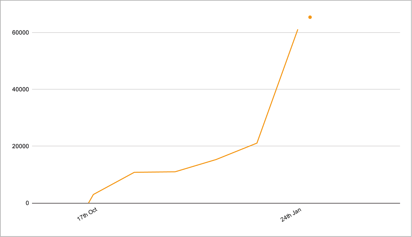
But now as we approach the 101st day of this campaign, or better, the $65th day, if we count in hexadecimal, we suddenly fund ourselves on the cusp of having enough money, thanks to 40,000€ coming in over the weekend!  Here is our happy little graph of progress:


The plateau has turned into a hockey stick :)

This means that we now have over 60,000 of the 65,000€ needed for the injection moulding tooling to be produced for us by Hintsteiner in Austria, and certainly enough for us to proceed with the next steps with them, to get the moulds produced.

From here to having the first injection-moulded cases in our hands will likely be close to 6 months, as the whole injection mould tooling process is not something that can be rushed.  The actual production of the tools takes a number of weeks, as the block of tool-steel is etched out using electrical sparks. 

But before we get to that point, we have to be really sure that we have the case design exactly right, because it is really, really expensive to fix later. Good industrial design and fabrication companies, like Hintsteiner, manage this risk by producing prototypes, and using trusted engineering partners throughout the process, meaning that you get what you want the first time.  This is one of the many reasons why we have chosen to go with Hintsteiner: We want the MEGA65 to be of the best possible quality.  Also, we want the manufacture process for the MEGA65 to all be easily reachable, manageable and controllable. Thus we have a cluster of partners all relatively nearby in Germany and Austria, so that we can produce batches over time, without having to worry about some disengaged partner on the other side of the world melting down our injection moulding tools because they thought we weren't going to order any more parts (or even just not enough parts to keep them interested).

This all requires close engagement with Hintsteiner over the coming months, which will be a focus for many of us on the team, as we look to get everything right the first time.  On that note, we are already thinking about the final set of port holes on the back of the case.  We are currently leaning towards having a cut-out for a user-port and cassette port -- even though these will require expansion boards of some sort that will connect in some way to the MEGA65 motherboard.  We'd be interested in hearing if there are any other holes for ports that people think we have forgotten -- because now is the time to pin this down, and it will be thereafter forever set in stone (well, in tool-steel ;).

Hardware is, as they say, hard, so we expect we will have more little challenges to solve along the way (such as having found out that there are some bigger up-front costs for the beautiful mechanical keyboards from GMK), but these are much smaller and more manageable, now that we have the funding for the injection moulding tools for the case mostly complete (there is still at the time of writing a few thousand Euro until the 66,000€ total is reached, for those who are interested in securing a position in the top 8 backers, in order to receive the benefits that come with that.  See mega65.org for more information.)

But in the meantime, lets all celebrate that this massive funding hurdle for the project has been dealt with, and that the path is now much clearer for us to proceed.