The MEGA65 has three FPGAs: One from Lattice in the keyboard, one from Xilinx as the main FPGA on the mother board, and one from Altera/Intel also on the motherboard. The Altera FPGA is programmed using a Trenz TEI0004-02 JTAG adapter on J17, while the Xilinx on is flashed using a TE0790 on JB1. The reason for these two adapters is a bit complex and historical, and influenced by which adapter works easily with the Xilinx and the Altera tools. But regardless of how we got here, it's our starting position.
Why this matters, is that some MEGA65 owners would really like to get a JTAG adapter connected to their MEGA65 for flashing and interacting with the main Xilinx FPGA. And this is where the problem comes in: Because of Chipaggeddon, Trenz will likely not have any more of the TE0790 adapters available for more than a year. BUT they do have the TEI0004-02's in stock.
Thus we would like to find a way to use the TEI0004-02 to control the Xilinx FPGA. We know that it won't work from in the Xilinx Vivado software, but it will work from the m65 command line tool, and also from m65connect on OSX and Linux. Windows may be a bit tricky, because we don't have a rock-solid way to talk to the USB JTAG adapters from in Windows, except to use Vivado. But even if Windows folks have to spin up a virtual machine running Linux, that will still in many cases be better than waiting a year or more. So, in short, there is good reason to do this little project.
First up, we need to get the pinout of JB1 and J17 from the MEGA65 schematics, and also making reference to the datasheet for the TEI0004 and TE0790 adapters.
Let's start with the TEI0004's pinout for its 10-pin header:
Pin 1 - JTAG TCK (output from adapter)
Pin 2 - GND
Pin 3 - TDO (input to adapter)
Pin 4 - Reference I/O-voltage from target board for JTAG and UART
Pin 5 - TMS (output from adapter)
Pin 6 - Reserved Output (May be used as Processor Reset in future software releases)
Pin 7 - UART RX (input to adapter)
Pin 8 - UART TX (output from adapter)
Pin 9 - TDI (output from adapter)
Pin 10 - GND
The TE0790 is a bit more complex, because it has a little CPLD that allows the pinout to be reassigned dynamically. So we need to know which profile it uses normally. For this, its easiest to work backwards from the MEGA65 schematics, where the pin assignments will be fixed.
Pin 1 - GND
Pin 2 - GND
Pin 3 - UART RX
Pin 4 - TCK
Pin 5 - 3.3V (but not connected, as I discover later...)
Pin 6 - 3.3V
Pin 7 - UART TX
Pin 8 - TDO
Pin 9 - Not Connected
Pin 10 - TDI
Pin 11 - Not Connected
Pin 12 - TMS
So, as we already knew should be the case, all the required signals are there: We just need to connect them to one another. For testing, I will just use a packet of header jumpers. If that works, we can design ourselves a little bitty PCB that will do the adaption.
So what we want is:
TEI0004 TE0790
1 TCK 4
2 GND 2
3 TDO 8
4 VCC 6
5 TMS 12
6 ---
7 RX 3
8 TX 7
9 TDI 10
10 GND 1
So that all looks good. I have an 8-pin header cable ready. To make my life easier, I will record which colour I am using for which signal:
TEI0004 TE0790
1 TCK 4 BROWN
2 GND 2 RED
3 TDO 8 ORANGE
4 VCC 6 YELLOW
5 TMS 12 GREEN
7 RX 3 BLUE
8 TX 7 PURPLE
9 TDI 10 GREY
I have removed the not-connected pin, and the duplicate GND lines in the process.
Testing that out, it looks like the adapter powers up, and I can even see the output of the serial monitor interface from the MEGA65, which is good. But JTAG communications don't work, nor does writing to the UART interface, so there is something odd going on.
In fact, if I even try to talk JTAG over it, then the machine goes all weird, resetting itself, and seeming to put random junk in memory.
This all suggests to me that I have likely got one of the UART and JTAG lines crossed... Now to figure out which. Perhaps the easiest approach here is to find the UART line, since it is the uart line from the host computer to the adapter, so I should be able to type some characters into a terminal, and see the correct line waggle. We are expecting it to be pin 7 or 8 on the TEI0004, on the blue and purple lines.
Without even going that far, I can see that the purple wire (UART TX to the MEGA65) is near GND, rather than floating at 3.3V. This is being caused by the TEI0004. So I am guessing I have the wrong pin... but double-checking everything seems to indicate that I do have the correct pin. The MEGA65 main-board has a 10K pull-down on the UART TX line, but that should not be so strong that the TEI0004 can't drive the line high.
I think I have figured it out: I was using pin 5 on JB1 for VCC, but this is not connected on the MEGA65. VCC is instead on pin 6. With it on pin 5, the VIO reference voltage would have been near zero volts, and thus we saw the problems we were seeing.
(Now, the astute reader might have noticed that I have pin 6 and not pin 5 in the table above, that is because I purposely changed it there after writing this, so that if anyone happened to glance at that to use it as a reference for themselves, that they wouldn't accidentally use the wrong wiring.)
... and funilly enough, with the correct voltage, both the UART and JTAG interface are now working: I can even do m65 -b mega65.bit to push a new bitstream to the MEGA65, or use m65 -S to take a screen-shot. In short, we have it all working :)
So now let's design a simple little adapter PCB, so that folks can do this, without having to have a bodge cable.
Done! and sent off to PCBWay for prototyping!
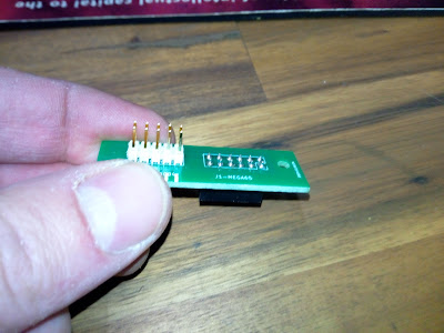
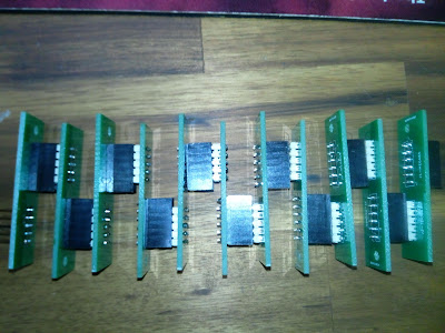
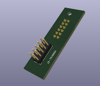
So it should look like in the following images when done:
From underneath, we have the 12-pin connector that goes onto the MEGA65's TE0790 header JB1. The big hole is supposed to line up with the 3mm hole in the MEGA65's PCB, so that if you want to secure it in place semi-permanently, this is possible. It also provides a nice visual indicator that you have it the right way around.
From above, we have the 10-pin header to accept the TEI0004.
And a couple of different angles, just so you get an idea of the whole thing. It is quite obviously very simple, hence why I was able to design it in about an hour, even though I had forgotten how to drive KiCad:
The particularly observant among you might have noticed that the TE0790 header is not lined up properly with the other two in the images above. This is a side-effect of the footprint I was using in KiCad having the pin numbers in the wrong order if I put it on the correct side of the board. So I designed it looking like this, i.e., with both on the same side, but with the pin positions actually correct. Of course, for assembly it doesn't make any difference at all:
Now its the annoying wait... PCBWay do have nice updates though as it goes through. Because the board is so small, I chose the largest batch size that would still give 24 hour build time (presumably because it fits on a single panel). So right now, it is already showing:
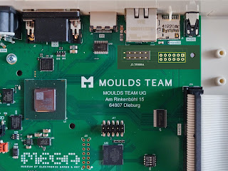
So while we wait for the boards and the connectors to arrive, thanks to AmokPhase101 we have mock-up images that will help you to see how it will fit together, and so that if you get one (or make your own), you can easily fit it into place:First, we have the upper right area of the MEGA65's mainboard, with the JB1 connector where the TE0790 JTAG adapter would normally sit. This is the 2x6 pin male header just to the left of the screw, and just below the microSD card slot, and above and right of the word "TEAM" in "MOULDS TEAM".

Finally, we can put the TEI00004 onto that connector, with the micro USB connector facing towards the front of the computer:
So that's everything, really, until the PCBs and connectors turn up, probably in a week's time, and I can test one out. I'm hoping that with it being so simple, I haven't screwed up one of the tracks or flipped pin numbers around or done anything else equally stupid (but that are all so easy to do with PCB prototyping). But those (mis)adventures will have to wait until the parts arrive...


