Just a quick note to say that we got the IEC (1541 drive / printer) port on the MEGA65 R2 PCB working today as well. This works well enough that we can even boot GEOS from a 1541 drive.
Of course, the native port of GEOS for the MEGA65 is much nicer, with higher resolution and MUCH faster booting: The GEOS load process takes probably less than 1 second.
We have yet to get C128/C65 fast serial working, but all the hardware is there for it. We will come back to this when we have time. The priority for the next two days remains to test the remaining functions on the R2 board, so that Antti and the crew have confidence of any potential changes required for what will hopefully be the production-ready revision of the board.
Okay, so we have the keyboard and disk drive ports both working already, so the next stop is to get the cartridge port working.
On this front there is hopefully not a huge amount that needs to be done. There have been a couple of pin re-assignments, as well as fixing a couple of issues that we knew about:
1. The FPGA pin for A15 has changed, which is easy to fix. In fact, for many purposes, it simply doesn't matter, because many cartridges only use the lower address bits. Anyway, it has been fixed now.
2. The /EXROM and /GAME lines that tell the MEGA65 to bank in ROMs from the cartridge are now proper input lines. On the first revision of the PCB these were connected to a two-way buffer that was really generally only used for output, so we had to periodically pause the bus and set the buffer to input, and read the lines. This can now be simplified, because the lines are pure input.
Fixing those problems didn't take particularly long. But cartridges were still not quite working. After some investigation, I found that there occasional errors reading bytes from the cartridge. Every now and then a byte gets read where some bits are changed from 0 to 1. It doesn't seem that they switch from 1 to 0, however. The R2 PCB has pull-ups on the address and data lines on the cartridge port, which the R1 did not have. Thus it is possible that there may be too much pull-up power, so I have just gone through and disabled all of that work for the R2 PCB.
Of course, that will take a while to synthesise, so I'll try to think about what else could be wrong. First I wanted to make sure that the cartridge port is not being run too fast: The dotclock is actually running at about 6.25MHz instead of 8MHz. The main clock is however running at 1.2MHz, which could conceivably cause problems.
The slow dotclock is because the pixelclock changed from 100MHz down to 80MHz, so I'll fix that while I am here as well. What is a real mystery, however, is that the phi2 clock is only 1/5 of the dotclock instead of 1/8th. I think I realise how this is happening now: The divider is /5 (0 to 4), instead of divide by 8, since the dotclock loop it sits in is counting dotclock phase changes, not clock cycles.
It turned out that the clock was not a problem, but the old logic for the R1 PCB to prime the data lines with charge (because of the lack of pull-ups), which meant that it would take longer for a line to get pulled low -- which is what we were seeing.
Then after this we found a problem where the cartridge_enable line in the CPU is not being enabled when requested, which meant we couldn't actually read the /EXROM and /GAME lines. So we have worked around this in the CPU initially, although the actual root cause is still not exactly clear, as the two locations that clear this flag should only be run under reset, and when the machine is in "secure mode" which is not the default.
After some hunting around this turned out to be caused by trying to keep compatiblity with the R1 PCB, which then confused the VHDL compiler with the way that I was using these signals as outputs as well as inputs. It actually took quite a few hours to get to the bottom of this problem.
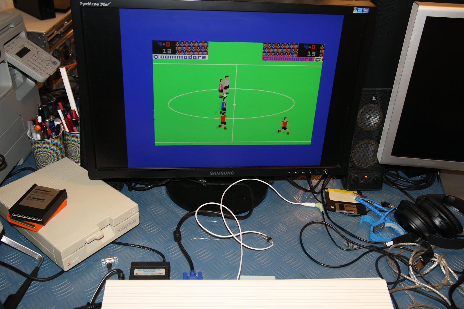
In the process, I also finally fixed the problem with some cartridges not working because they only pull /EXROM or /GAME low briefly on reset, typically with a capacitor. The boot ROM now pulls the cartridge reset line low for a little while before exiting to boot, so that such cartridges present their ROMs. This enabled such cartridges as the Epyx Fastload cartridge and Power Cartridge to begin to work. There may be features in them, and many other cartridges, that don't work, but we are getting to the point of having quite a number of cartridges working. Even the Ezyflash works now, although it is mostly rather useless to use a flash memory cartridge on a computer that already has an SD card for bulk storage.
Anyway, this has let us test the cartridge port enough to have confidence that it works physically, and the rest of the compatibility improvements in the future should need to be software/VHDL only.
So, in the last post we reported that we had the keyboard mostly working. In the meantime, we managed to figure out the remaining problems with the communications protocol, and map the remaining keys.
As a result every key now works as it should, the clicky lock keys illuminate their LEDs, and behave as expected. All of the dedicated lines for special keys, like the left and up cursor keys that live outside of the keyboard matrix on the C65 are also correctly handled.
Suddenly it started feeling a lot more like a computer, now that we could type on it and interact with it. We could do long-press on RESTORE to get to the freeze menu (reset is now only via the dedicated reset button the left side of the computer).
It really feels very nice. The work we put into having sub-millisecond latency on the keyboard has really been worth it. There is absolutely no perceptable delay, and it just works as it should. The indicator LEDs for the LOCK keys work perfectly, and with their clickiness and different tactile resistance, you know with certainty when you press one. In short, we are really happy with the result, and hope that everyone who uses a MEGA65 will enjoy it as much as we do.
So, now onto getting the cartridge port working...
Ok, so now that I can program the three FPGAs that are in the MEGA65 R2 board and keyboard, it is time to try to get the keyboard working.
The keyboard has an 8-pin interface, which we can define however we like. The same pins are also used for the JTAG interface when programming the keyboard's FPGA. So to simplify things, I'll use the same pin names as with JTAG.
The protocol will be a simple bit-shifter that shifts out the state of the 70 keys on the keyboard, and also allows shifting in of bits of data/control from the MEGA65 itself, e.g., to control the LEDs. This can be done easily with four lines, just like JTAG: Clock, synchronisation signal, data in and data out. The MEGA65 will simply run the clock, and periodically assert the synchronisation signal, and then read in the bits of keyboard matrix, and at the same time on each clock tick send out the bits for the LED control.
The keyboard will provide the state of the 70 keys, complete with simulating the held status of the caps and shift-lock keys -- that is, the keyboard will internally keep track of the state of those two keys.
To plumb this through I am moving the layer that handles the widget board that we designed for the Nexys4 boards from deep down to the outermost layer of the VHDL, so that it can be replaced with alternatives. The new keyboard will then be implemented by creating such an alternative.
This has now been done, but I now have to debug it all, because not surprisingly, it didn't work first time. Main problem is we don't have an oscilloscope here in the cellar. So a bit of frantic searching was required for one that was: (a) near by; and (b) not too expensive. There were some nice ones for <100 Euro, but not near by, and since we don't have that long with me being here, we didn't really want to have to rely on multiple days of postal delivery. We did in the end find a nice 1987-vintage Tektronix 2430A from a University student here in Darmstadt, and with a new probe ("Tastkopf" is my new German word for the day) we now have a suitable setup for probing pins for 220 Euro:
So, the keyboard protocol should have a clock of ~2MHz and syncrhonisation pulses at ~10KHz or so on the keyboard connector, but neither are visible. This makes me suspect that the plumbing through from the Xilinx FPGA through the MAX10 to the keyboard connector is not right.
To verify this, I have created a test bitstream for the MAX10 that routes the keyboard clock signal from the Xilinx to one of the two on-board LEDs, and then another for the Xilinx FPGA that puts at 40MHz clock on that line, without any conditional logic that could be messing things up. Hopefully with that I should see the 40MHz signal on the LED pin.
After a bit of fiddling, I have come to the conclusion that going through 2 FPGAs and a cheap oscilloscope probe and into 1987-era oscilloscope is not that conducive to seeing a 40MHz clock. So I instead made the MAX10 wiggle the line at varying speeds, which confirmed up to about 10MHz is easy enough to see, and there is a weak signal at higher speeds. So then it was a case of adjusting the Xilinx test bitstream to produce a signal in the right frequency range, and tada! I had a nice signal.
So now the next step is to pull the new keyboard controller into the Xilinx test bitstream, so that I can see if I can see the signals being produced by that. Okay, so have that in, and pleasingly, I can see a signal. However, it is only about 20Hz, instead of ~2MHz. Ah, no, actually it is in fact ~1MHz, which is fine:
To give an idea how tricky this scope is in the wrong time-base, here is exactly the same signal, but shown at the wrong time base. The only real hint that something is wrong is the ripple in the signal. Of course, someone who was actually educated in electronics rather than picked it up as they went along would probably have spotted that, but oh well. I just have to get used to this oscilloscope not giving a clear indication when it is showing low frequency harmonics if the time base is way out.
Ok. So that's one problem down. Now to see if that signal shows up on the relevant pin of the keyboard connector: Yes, nice clear 1MHz clock on pin 3. Probing around the connector, I can also see a signal on pin 5, that looks to me like the LED control signal from the computer to the keyboard, which is also in the right place. The synchronisation pulse is also visible on pin 4, and there are signals on pins 7 and 6, although I am not yet sure if they are correct. It is possible that they are wrong way around.
To check that pins 6 and 7 are correct, I have disconnected the keyboard. That way only the signals from the FPGA should be visible. Doing so leaves the signal on pin 6 visible, and the signal on pin 7 disappears: This is correct. So it looks like we now have communications with the keyboard possible, from a physical sense. So now to debug the communications.
First step is to see if the synchronisation signal on pin 4 is being captured or not. This signal has a pulse width of only ~1usec. This SHOULD be enough, because the keyboard FPGA runs its internal clock at about 12MHz, so it should see the signal for several clock-cycles. To test that it is being captured, I have configured one of the LEDs to increase in brightness each time a TMS signal is seen. It seems that it is not captured.
Since the signal should be wide enough to be captured, I am now wondering if the pin assignment is wrong, or some other similar problem. To test this, I will have the keyboard FPGA route the TMS signal back out onto the TDO line, so that I can see what it thinks it is directly. If it comes through fine, then I know that there is a problem with the VHDL logic, rather than the clock capturing per se.
Well, a lot of fiddling around has established that I don't seem to be able to read the JTAG pins as inputs from in the Lattice CPLD. I have made sure JTAGEN is low, so that the JTAG interface is not being taken over by the JTAG system, but I still seem to only read fixed values from the JTAG input pins. Apparently this is the default behaviour according to http://www.latticesemi.com/en/Support/AnswerDatabase/3/0/4/3043. So I can apparently set a flag to make them usable, but I need to make sure that doing so doesn't effectively permanently disable JTAG, thus preventing me from ever re-flashing the things. That would be bad. Anyway, it does at least explain the behaviour I am seeing.
There are a few potential solutions here: First, I try to figure out how to switch the JTAG pins safely. Or alternatively, we do have 3 true GPIO lines on the connector, and so I could just write a protocol that uses only 3 pins instead of 4 to communicate with the keyboard. Then it is a question of what protocol to use.
Probably the easiest is to switch to a 3 wire protocol, and use a stretched clock signal as the sync signal. That is, if the clock pulse is longer than, say, 2usec, then it is a sync signal. That way the rest of the protocol can remain unchanged.
We can have the keyboard read and write bits on the rising edge of the clock, and the Xilinx FPGA can read and write on the falling edge, so that everything stays nice and simple.
As with everything VHDL, this has taken a little longer than expected, and involved the usual cycle of me thinking I can get away without a test harness, and then eventually making one anyway, when I hit some inscrutible bug. But I now have a 3-wire interface that uses a stretched clock pulse to mark the synchronisation.
One fun thing I found while doing this, is that having the keyboard protocol running on the keyboard cable while trying JTAG program the keyboard generates enough cross-talk to cause trouble with the JTAG verification process. So mental note to de-configure the Xilinx FPGA (or have it stop the keyboard protocol) before trying to flash the keyboard FPGA.
Better would be to make the dip switch that connects the keyboard to JTAG to also stop relaying the keyboard protocol pins through. That means programming the MAX10 again, which is usually not much trouble now. This time however, it tried to claim that the programming cable was not connected, when in fact it was. The problem turned out to be that jtagd got confused, which was fixed by killing jtagd, so that it would restart on the next programming attempt.
Excellent! I now have a blinking keyboard led (which is what the test Xilinx bitstream is supposed to do), and I can stop it blinking by enabling JTAG to the keyboard (which is what I just attacked), so I should now be able to easily flash the keyboard again.
Now, I said the LED is blinking, and it is blinking. However it should be the drive LED, not the power LED that is blinking (which is oddly the one nearest the drive). Also, it should only be flashing RED, not with the occasional flash of blue. And the other LED should be staying off. However, such naughty things are happening.
Swapping which LED blinks should be nice and easy. Working out the cause of the flashing is another thing altogether. My best guess is that there is some clock glitching due to crossing clock domains etc. This should be fixable by debouncing the clock. Indeed, debouncing for a single cycle seems to be enough to fix it.
Now the colours are stable, but the LEDs are appearing green instead of the red that they are being instructed to be, so I'll need to look into that. But first, I want to have a clear indication of when the computer is or isn't connected to the keyboard. So I'll implement a bit of disco lights, maybe in police light style, that indicate when the computer isn't talking to the keyboard. This should only ever happen in the first fraction of second at boot, which I will mask. So basically if the police lights come on, you have a problem and need to pull over and sort it out.
Right, now back to the important business of getting the LEDs functioning properly for normal purposes, and working out if there is still any funny clock stuff going on. The reason I suspect clock funniness is because the wrong colour, which makes me worry that the clocks are being counted at half rate or so on the keyboard side, since red is in the first 8 bits, and green in the second. Or alternatively there are 8 bits being stuffed in at the beginning of each round of communications, which is causing the shift. I'll have tthink about it for a bit.
See: The LEDs can blink, just in the wrong colour.
But what is also nice now, is that the keyboard is responding with information about which keys are being pressed. This should be super responsive, because we get a complete update of the keyboard state every ~0.1 milliseconds, so the delay of the keyboard protocol should be really negligible.
So now to plumb it all in, so that the MEGA65 starts trying to use the keyboard. We know that the matrix will all be messed up initially, but that's okay. First step is simply to get the key presses received and interpreted.
Okay, so, now I can detect when some keys are being pressed, but not all of them. A bit of hunting found a stupid bug in the code that handles the key presses, which was causing all key presses to be interpreted as only one of the first 8 keys in the matrix.
Ok, fixed that, and now the keyboard decode accelerator at $D610 shows various ASCII codes of keys I am pressing (all messed up, because the matrix is not correct, yet), but our OpenROM BASIC is behaving as though there is no keyboard. A bit of poking around has found that this is because it thinks the joystick is active on all 5 inputs. We had this problem with the R1 board due to lack of pull-up resistors, but that was supposed to be fixed. What is weird, is that it is only one of the joystick ports doing this. I am now trying to work out which joystick port it is, and whether it is missing pull-ups or something else.
Hmm.. Oscilloscope is claiming that there is 0V on every pin of both ports. This new PCB does have a "5V enable" for the joysticks, which is controlled by the MAX10 FPGA, so I'll have to take a look at that. After some chasing around, I found and fixed a couple of stupid typos on my part, that mean that I was enabling on the wrong pin. This was complicated slightly by the fact that the voltage control for the joystick port on the R2 boards already has a small patch on it. Also we confirmed that the pull-up resistors were forgotten from the joystick lines, which is a bit annoying, but easy enough for us to fix. It's just a nuisance, because all 25 series boards will need to have ten surface-mount resistors fitted, and then tied to VCC. That's quite a few hours work, in all likelihood.
Now, back to the keyboard, all that fuss about the joysticks was so that I could stop the joystick lines interfering with the keyboard scanning. I'll have to implement a register that lets us connect and disconnect the joystick ports internally. I had done this previously for the R1 PCBs, and it is just a case of resurrecting it.
Ok, so I have done that, can can see the joystick inputs disappear -- but there are still some funny things to solve: Pressing keys doesn't reliably set the bits in the bytes, and indeed the bits float around a bit. This took quite a while for me to realise that I had de-glitched clock edges only partially. Once I realised that, I was able to sort that out.
Then the next funny problem is that some of the first few bits are still coming through as though keys are pressed -- even though I can see on the oscilloscope that the input line stays steadily high. Also, there seems to be a synchronisation problem with the LED colour receiving. I think that it is probably reading one clock or one edge early or late. The two problems may even be related directly, but that will require some investigation.
I am now invetigating the LED problems. First, I have fixed a problem with the PWM brightness control. Now I am trying to work out if there is a shift in the bits of data compared to where they should be. The data consists of 4 x 24 bits for 8-bit RGB channels for each of the LEDs. This is 96 bits in total.
The first 8 bits should be the red channel for the first LED, but seemingly do nothing. So now I am working my way through systematically to figure out what is going on. This requires about 3 - 4 minutes as I test each byte to see what it is being mapped to. Ok, so the second 8 bits are also not seeming to do anything. Ok, finally hitting where bits are doing something:
Bits 0 - 31 = nothing
Bits 32 - 39 = Blue channel for the second LED from the left.
Bits 40 - 47 = Green channel for the second LED from the left.
bits 48 - 55 = Red channel for the second LED from the left.
Hmmm, it seems to be backwards. Also note that 128 bits (total frame length) - 96 bits = 32 bits, which is suspiciously the size of the region which does nothing. A closer look reveals that I am sending the bits indeed in reverse order.
Ok, time to reverse the bit order then, and see if that fixes it.
Hmm... Closer, but still something odd. I requested a red solid LED for power and blinking green drive led, and I have instead a blinking red LED and solid green one. They are also on the wrong LEDs, but that is really easy to fix. I'm trying now to make the power led solid purple, and we will see what that does. Most strange: I now have a blinking purple LED, even though the logic for the purple LED should have it solid on. Found the cause of this: I had for some deranged reason in my test harness decided to make the power LED blink and the drive LED solid. Anyway, it's nice that that is now out the way. The LED control is now all perfect, with C65-style green power and drive LEDs.
Now, back to the keyboard. Plenty of fun adventures to be had here, as I have chased down a variety of fun bugs. The bit order was being reversed here as well, but then the big problem was that initialising signal values doesn't seem to work on the Lattice CPLD we are using. It's probably a known situation, but it wasn't known to me until now.
So FINALLY I have the keyboard communications more or less working, and now just have to map the ~80 keys to the correct matrix order. I have the schematic for the keyboard, as well as the C65 keyboard matrix from section 2.1.2 of the Commodore 65 Specifications, and I just have to match them all up. Unfortunately the keyboard schematic for the MEGA65r2 doesnt show (or at least I couldn't find) the key number to keyboard position mappings, so I have to figure these out for myself.
I've started with SHIFT LOCK, because the lock keys are clearly marked on the schematic, and then with RUN/STOP and ESC because I can also deduce where they are. If my hunches are confirmed, I will be able to fairly quickly match up more keys. So, this worked in so far as I could indeed tell that I am pressing the correct keys. However the matrix mappings seem to be wrong.
Fortunately I implemented the on-screen-keyboard for the MEGAphone, which lets me see in real-time exactly which keys are being pressed. While this wasn't its original purpose, we can always pretend it was made for this purpose, for which it works fantastically, and looks pretty nice while doing it.
RUN/STOP should be key 63, but pressing it causes D to be pressed, as can be seen above, which is key 18 (column 2, row 2).
ESC should be key 71, but works as A, which is key 10.
SHIFT LOCK (key 15) works as key 66
Ah, in all cases they add up to 81! That means that the bit order is just reversed, which we can easily fix. Oddly, trying to reverse the bit order didn't fix it, but making the key numbers be 81-(key number) has worked, so I am not going to worry too much for now. So now to implement more of the keys.
Getting the vast majority of the keys correctly assigned took about 2 hours of iterating through, but in the end, we have most of the keys right. So we can finally type some things in, and even load programs again. However there are a number of keys that are behaving oddly, which we will have to fix up. But as this post is already half a mile long, I'll stop here for the moment.
Ok, the keyboard test bitstream is currently synthesising, so I though I would look at another important sub-system in the meantime: The SD card interface.
The R2 PCB has both an SD card and microSD card interface. As I have mentioned in a recent post, the microSD interface goes through the MAX10, which complicates things a bit. Also, the pre-series cases are quite tight around the microSD cards. So, for both these reasons, we will concentrate on the full-size SD card slot.
So, to begin, I am using my FPGA pin identification framework to work out where everything goes. What I really need to know is the exact model of SD card connector we are using, so that I can verify that everything is correctly connected.
First up, check if we have VCC and GND
The signals we need are:
Data Out (DO)
Data In (DI)
Card Select (CS)
Clock (SCLK)Power (VDD)
Ground (VSS)
Now to see if they are on the correct lines in the current bitstream. I'll use my test bitstream that puts a unique bit sequence on each, so that I can see which is which.
VDD - Correct at 3.3V
VSS - Correct at 0V
DO - FPGA pin #10
SCLK - FPGA pin #8
DI - FPGA pin #11
CS - Stuck at about 2V
The CS line looks to be the problem here. Hunting through, I have found that I hadn't plumbed that line through properly. So a bit of poke and fiddle, and it suddenly was working :)
Having the SD card working is super helpful, as it makes it MUCH easier to load things for testing.
Also, it is nice seeing other bits and pieces obfviously working, now that we can get as far as booting. In particular, the internal floppy drive now does its spin and seek during the boot sequence. A happy piece of progress after a lot of preliminary work over the past few days.
Okay, so we have the main Xilinx FPGA and the utility Altera MAX10 FPGA able to be programmed on the MEGA65 R2 mainboard now.
That just leaves the Lattice FPGA in the keyboard to program.
First step is to program the MAX10, so that can route the JTAG to the Xilinx and Lattice FPGAs. This done using the Quartus tools, but remember to hold the reset button in on the MEGA65 mainboard, as that asserts the JTAGEN line on the MAX10. The Arrow FPGA programmer module needs to be plugged in to do this. Then the normal Quartus programmer interface can be used (but remember to first have fixed the problem with the Arrow FTDI USB driver setup by following these instructions).
Actually, we simplified this by making a program.sh script, that does the programming itself -- but you still have to hold the reset button in.
Second step is to program the Xilinx FPGA, because our current MAX10 firmware connects the JTAG interface to the Xilinx FPGA until it asserts the FPGA_DONE signal, i.e., has been programmed. This requires using the TE0790 cable, and if you have the Arrow cable plugged in at the same time, you might need to run fpgajtag with the -s option to specify the serial number of the cable to uses. If that is successful, the MEGA65 will now have the friendly blue boot screen visible.
That leaves the third step. Here we had a bit of fun dealing with a JTAG latency problem with the bypass through the MAX10 FPGA as well as the latency of using a conveniently long keyboard cable. We thought about making a custom programming cable, but would prefer to keep things simple, so decided to explore how we might defeat the latency problem. Setting the "Programming Speed Settings" in Lattice's Diamond software's programming utility managed to make it work for us, and we were then able to flash the keyboard. Yay!
It should be possible to make the keyboard flashing work via the Arrow cable instead of the TE0790, by bypassing the JTAG signals to the appropriate pins on the Arrow programmer. In fact, it should be possible to program all the FPGAs from that one interface, and even redirect the serial debugger interface there, although the serial debugger is perhaps best left where it is, so that the problem with the MAX10's programmer needing to be in the mode where it has no serial ports mapped (the root cause is a limitation in the Linux kernel with regards to having USB devices controlled by two different drivers at the same time). However, when I tried to do this, it didn't really work. So we'll just ignore that for now.
What we will do, is make the JTAG bypass of the MAX10 dependent on a dip-switch, so that we can talk to either the keyboard or Xilinx FPGA as required, e.g., so that we can flash the SPI flash so that it automatically boots up on power up. This I have now, done, so we can flash the configuration for the Xilinx FPGA as before, using a command line like:
./megaphone-write-flash.sh bin/mega65r2.mcs
This works even though it is the MEGAphone targeted script, because the MEGAphone and MEGA65 R2 mainboards both use the same serial flash chip for storing the configurations.
But before we do that, we really need to flash our updated MAX10 bitstream, because the initial one that is there stops listening to JTAG when the Xilinx FPGA is configured. This means that we need a nice easy way to write to the flash in the MAX10 FPGA, and this turns out to not be that simple.
The MAX10 FPGAs have built-in flash, and the flashing tools don't have the means to automatically make a bitstream that allows writing to the internal flash. This is annoying, since the Xilinx tools do this really nicely, even when writing to external flash. Instead from what I can gather, you have to build a NIOS2-enabled bitstream, that also has the flash memory connected to the NIOS2 processor, so that the flashing program can instruct the NIOS2 CPU to do the flash memory accesses. This means I have to figure out how the whole IP core connection stuff in Quartus works.
After talking to Antti, it turns out there is a really simple way to flash the internal flast in the MAX10: Simply program with the .pof file instead of the .sof file. This works nicely, so I have made a script flash.sh in the MAX10 repository for this.
So, let's go over all of this from the top, now that we have the various tools at the ready:
0. Plug in both the TE0790 and Arrow programmers to the board.
1. If Xilinx FPGA is already configured, then unconfigure it by running fpgajtag -s <serial number> <a valid bit stream> and pressing control-c as soon as it says "starting to send file".
2. Hold the reset button in to put the MAX10 into JTAG mode, and run the flash.sh script to flash the MAX10 FPGA with our bitstream.
3. Release the reset button, and ensure dipswitch 1 is in the off position, to select the Xilinx FPGA for JTAG bypass.
4. Run ./megaphone-write-flash.sh bin/mega65r2.mcs to flash the Xilinx FPGA.
5. Switch the dipswitch 1 to the on position, to select the keyboard's Lattice FPGA, and unplug the Arrow programmer's USB cable from your computer.
6. Run program.sh from the keyboard cpld directory to program the keyboard.
After this, all three items should be finished flashing, so that turning it off and on brings it to the same state.
Now, finally, we can start trying to move forward with actually bringing up the functionality on the board.
Yesterday with the super help of Martin, one of the MEGA members, we spent the day in a studio to get much nicer looking photos of the new cases, keyboards and motherboards -- and of course whole assembled pre-series machines.
I have a saying "filming takes longer than longer than you think", and indeed this held true. Apart from a 3:30pm pizza break, it was about 9 hours of work to get images of the MEGA65 pre-series prototype machines, and also of the proof-of-concept handheld. The handheld was a real varmint to photograph, because it is all black, see-through and VERY reflective.
We wanted to produce material that could be used to replace various renderings and other bits and pieces on the mega65.org website. And in this regard, we are very happy, and have indeed removed practically all rendered material from the website, to instead show mostly only real physical hardware.
There isn't really much more to say, other than enjoy the nice photos of the MEGA65!
I mentioned recently that I have been struggling with getting the Arrow FTDI-based JTAG programmer working with Quartus for programming the MAX10 on the MEGA65 R2 main board. The problem is that I could get Linux to either disconnect EVERY ftdi device, or none. This sent me down a bit of a rabbit hole that warrants a few comments:
1. The 51-arrow-programmer.rules file was completely wrong and worked only through sheer luck. The file contained Windows line termination characters, which caused all lines except the last to be ignored. That last line happened to be the one to instruct the FTDI_SIO driver to disconnect. As a result it would ALWAYS disconnect EVERY FTDI-based serial adaptor -- including the ones I needed connected.
2. I read through lots of udev documentation and related material, and while it SHOULD make it easy to do this kind of selective work, it doesn't because by the time the FTDI_SIO driver thinks about whether to be connected, all the useful identifying information (like vendor name and serial number) have been stripped out.
3. In the end, I used the RUN directive in a udev rule to run always, just like in the broken rule file provided, but to have it run a little script I wrote that checks for the last inserted FTDI adapter that has "Arrow" as the vendor, and then work out the serial port kernel ID, and disconnect that.
Here is my rules file:
# Arrow-USB-Programmer needs to be disconnected from ftdi_sio driver RUN="/bin/sh -c '/etc/udev/ready_arrow'"
And here is the contents of /etc/udev/ready_arrow: #!/bin/bash dmesg | grep `dmesg | grep "Product: Arrow USB Blaster" | tail -1 | cut -f3 -d' ' ` | grep ftdi_sio | cut -f3 -d' ' | cut -f1-2 -d: | tail -1 | sudo tee /sys/bus/usb/drivers/ftdi_sio/unbind
And it works like a dream. So now I can insert the USB adapters in any USB port, in any order, and have them all in the correct state.
So now I can finally get back to what I was trying to do, which is to try my new MAX10 firmware, to see if I can get the serial monitor interface working on the MEGA65 R2 main boards...
Ok, so we have managed to get the thing to power up, but when I went to test further, I found I wasn't able to establish communications with the serial monitor interface. Quite likely I have the RX and TX lines swapped or something equally stupid.
To fix this, I'll need to resynthesise the whole thing, which will take ~30 minutes. However, it would be great to be able to test things faster than that. A very simple FPGA program can synthesise in about 3 minutes, which is much better. Since we will likely be testing a pile of stuff over the coming days, it is worth making such a program, so that we can quickly iterate things.
Ok, so I have done that, and then realised that until we program the little FPGA that handles IO routing, we can't actually even use the UART monitor. To make life more fun, that FPGA is an Altera/Intel MAX10 -- this means a completely different tool set compared with the Xilinx main FPGA. So time to download 6GB of software, install it using 15GB of disk, and then learn how to use quartus for the first time.
After considerable fighting, I think I am on the way. Instead of an .XCF file for constraints, it uses a .QSF file, which has syntax that is not totally different to that of the XCF files. For example to assign the four pins for the monitor UART (2 to the Xilinx FPGA and 2 to the JTAG connector), the following does the trick: set_location_assignment PIN_A5 -to te_uart_rx set_location_assignment PIN_B4 -to te_uart_tx set_location_assignment PIN_J10 -to dbg_uart_rx set_location_assignment PIN_K10 -to dbg_uart_tx
So in theory that should be enough to be able to connect logic to the pins. We should in theory just need to connect te_uart_rx to dbg_uart_rx and similarly for the *_tx lines.
I have also put it under source control, although I am sure for now that I have included all manner of build artefacts, rather than just the source files. Perhaps a willing volunteer with some experience with quartus can provide a pull-request to sift them out and create an appropriate .gitignore file. The repository is at https://github.com/MEGA65/mega65-r2-max10
Now the only problem is we are out at a studio to get photos of the MEGA65 pre-series units, and didn't bring the programmer or power adapters with us, that would let me test it.
But in the meantime I can try to solve another problem: The Quartus/Arrow USB drivers to use the programmer for the MAX10 have the annoying side effect of taking control of all FTDI devices with the same USB ID. This is annoying because the adapter for the Xilinx FPGA gets picked up by it, which prevents it from being available to connect to. The problem is that the udev rules file seems to ignore the serial number and vendor fields, so I can't just make it handle the two differently that way.
Digging around on the internet, I found this nice summary of things: http://hintshop.ludvig.co.nz/show/persistent-names-usb-serial-devices/. The nice bit here is the info on how to create symlinks to devices. In theory, I should be able to use that to modify my rules file to see when it picks up one or the other.
But I fear that the problem is that the same driver gets used by Linux for ALL devices with a given USB vendor:product tuple, so I might need to change the tuple for the Arrow programmer board.
Digging further, this looks like it might be a problem of how the detection works, in that all variables have to be considered at a single level of the USB device specification (https://askubuntu.com/questions/978485/udev-rule-with-serial-for-ttyusb-not-working). That article suggests doing the tying based on which physical port things are connected to, which could work for me, and also suggests that it should be possible to do it on the basis of serial numbers. I might need to simplify the rule to just look at the serial number and nothing else. Again, I'll have to wait until we get back to where we have the adaptors.
Ah, reading further in the rules file, it seems that part of the problem is that the rule unbinds the FTDI SIO driver when the rule is triggered, which would cause it to unbind any existingly connected device as soon as an Arrow programmer is plugged in. The question arises in my mind, that I am not actually sure that it is a problem that the serial driver remains connected. Again, something else to test later today.
What I can do in the meantime, is to get the rest of the pins for the MAX10 labelled in the QSF file, so that I can begin implementing the rest of the connections, such as to the keyboard.
So, having gone through that, there are a few interesting things that Antti and the folks at Trenz have included:
1. The microSD card slot also doubles as a JTAG programming/debugging interface for the MAX10 FPGA, if you hold the reset button on the side of the computer in. This means with a funky adapter it will be possible to program the MAX10 without even opening the machine.
2. The MAX10 is able to control the JTAG debug interface to the Xilinx FPGA and keyboard, so the same interface can be used to program the Xilinx FPGA from outside as well.
3. Four dip switches for setting things about the machine, e.g., defaulting to PAL/NTSC or keyboard nationality.
4. 256-byte serial flash with globally unique ID, e.g., for seeding the mac address or serial number identification of the machine.
5. 16KB serial flash for storing other things, if we have need. It might be possible to increase this to 128KB, so that a complete ROM could be stored there.
6. A real-time clock and battery, which we can do a bit of magic with, so that the CIA RTC registers get initialised with the values from the actual RTC. It would even be possible for us to make writing to the CIA RTC registers cause the actual RTC to update.
7. The power to the PMOD expansion connectors can be turned on and off for hot-swap.
8. 12-pin debug/expansion header connected directly to the MAX10 FPGA.
But, back to the point at hand, we need to work out which pin connections we need to setup in the MAX10 FPGA. I think the list is:
1. Tri-state Xilinx FPGA reset and related configuration lines
2. Enable 5V power output to joysticks and expansion port.
3. Connect Monitor UART interface between Xilinx FPGA and TE0790 connector.
4. Connect Keyboard connector to Xilinx FPGA.
5. Connect Xilinx FPGA JTAG debug interface to TE0790 connector.
6. Connect microSD card to Xilinx FPGA.
7. Connect reset button to Xilinx FPGA.
8. Disable power save for VGA VDAC.
Most of these are simply straight-through routing of signals. However, the microSD card interface is a bit annoying, because there is no matching set of pins between the Xilinx FPGA and the MAX10. This means we will need to implement an SD card controller in the MAX10 and relay the data at the sector level -- or get the R3 PCB to have the lines to connect it directly to the Xilinx FPGA.
Anyway, that's all we can attack for now, until we get back to base in a couple of hours.
FINALLY I have arrived in Germany with the MEGA65 crew, so that we can start bringing the MEGA65 R2 PCBs to life.
Here is the board in its case, together with the JTAG programmer, which we need to plug in to be able to program the FPGA:
The problem was when we first plugged the JTAG adapter in, it didn't have any happy lights. But a quick message to Antti confirmed that we needed to set the dip-switches correctly, as shown below. Then it powered up fine, as we can see below:
Then at this point, we were in a position to try the bitstream that we had previously prepared. This bitstream won't make everything work, but has the parts that are common with the first revision, primarily the VGA output, sound output and joystick inputs. And, joy of joys, it worked, with a nice display:
It is showing our open-source C64 ROMs, because that is now included in the bitstream as the default boot mechanism if there are no SD cards inserted.
The reset button has also been corrected in the R2 board, so that it resets the CPU instead of causing the FPGA to reflash.
Ok. So that's the first step of livening done. Now to try to get the joysticks and souund working...
Things are getting exciting again! We have the first two samples of the second revision of the MEGA65 main board. This incorporates fixes to all the known problems of the first board, as well as a bunch of pleasant extras.
But first, we are super appreciative for everything that Antti and the rest of the crew at Trenz Electronics
have done to get us this far. Without their dedication and kind
support, we would not have a MEGA65 mainboard at all, let alone one that
is so nice for all that we want to do.
Now, onto the first pictures:
So, there are quite a few changes from the first revision:
1. Power cord now comes in from the back, instead of from the side, which makes things just nicer and neater.
2. Cartridge port cut-out is now wider, to allow even the fattest cartridges to be more easily connected.
3. VGA and HDMI connectors now have enough space to be both connected without causing trouble. It will in principle be possible to drive the two independently with different pictures, when we get that far. This is more of concern to those who want to be able to run a C128 core with simultaneous 40 and 80 column displays.
4. Missing pull-ups on the joystick ports, cartridge port and floppy connectors have all been added.
5. SD card slot and microSD card slot both added, which is very welcome as in the rush to get the first revision ready, the SD card was left as an "after factory add-on", i.e., had to be hacked on. The MEGA65 will be able to use both SD cards at the same time, with dual-card support already in the VHDL, and will come in due course to the Hypervisor. For now, it just tries the second slot if there is nothing found in the first slot. The internal one is a full-size SD card, so strange SD cards, like those ones with Wi-Fi onboard should be possible to use.
6. PMOD GPIO connectors that allow internal expansions. We expect, for example, to be able to make an adapter that will allow the installation of a cellular modem, 8266 Wifi or RN52 bluetooth adapter, based on the work on the phone/handheld version, thus allowing wireless networking for the desktop MEGA65. This is just one of the many little synergies that come from working on both versions at the same time.
7. Dual power connectors for internal floppy drives. Again, we forgot in the rush last time to include any of these.
8. On-board real-time-clock (thus the battery holder) so that you can easily remember just how many years of happy use you have extracted from your MEGA65.
9. The C64 and C65 compatible keyboard connectors have been replaced by the 8-bit 8-pin serial interface to the MEGA65's custom mechanical keyboard. It will be possible to make an adaptor to still use a C64 or C65 original keyboard that connects to this interface.
10. Reset button tells the CPU not the FPGA to restart, i.e., without losing the contents of RAM. In short, it will work as a proper reset button.
11. Addition of a 2nd "Little Brother" FPGA that can be used to recover from bricked FPGA configuration, without having to even open the case. This will also make it much easier to flash updates onto the MEGA65 for end-users.
12. Addition of support for an internal speaker on J19, for when you don't have a monitor with speakers.
13. Addition of an extra I2C bus for other expansion peripherals on J18.
14. Fits our wonderful new cases just fine.
15. Lots of other little and not so little fixes.
Now the biggest problem is I don't get to Germany until Saturday, so have to wait impatiently in the meantime before I get to play with them :)
What I have done, though, is create a mega65r2 target in the VHDL source, which Antti has already confirmed gets a working video display on the VGA output.
This is another of those rather long "whodunit" type posts, where I basically document the process of solving a particular problem.
When we started designing the MEGA65 phone, we did a lot of searching to find a way to give it really nice sound on the internal speaker, both so that games and demos would sound great, but also so that it can ring really loud. There is nothing worse than a phone than rings too quietly to be easily heard.
So we were pretty happy when we found a 40mm diameter and <5mm thick 2W speaker that claims peak levels of close to 100dB. We coupled this with a nice amplifier chip that can in theory deliver enough power to make good use of this speaker. Privision was also made for stereo, although the first prototype device will have only one speaker installed, to keep life simple.
The amplifier is an SSM2518 I2C controlled digital amplifier, which means we have easy digital control via the I2C bus, both for settings, and also for setting the volume level. We already have the I2C bus working, and can read and write its registers at $FFD7030-$FFD7042. Also, the audio cross-bar mixer has outputs setup to feed this amplifier. So in principle, we have all the ingredients we need to make it work. Now is the time to actually get it working.
First, let's look at the I2C configuration that we need. There are 19 registers, only a few of which are important to us, and of those, only certain bits are important:
$FFD7030 - bit 0 = Software master power-down, and must be 0 for normal operation.$FFD7030 - bit 5 = "no BCLK". If 1, then MCLK is used instead of BCLK to generate the sample clock. Thus we want this 0, so that we can just have BCLK, and, hopefully, require one less pin.
$FFD7030 - bit 7 = software reset, and must be 0 for normal operation.
$FFD7032 - bits 5 - 6 = Serial Data Format. 01 = left-justified samples, which is what we want.
$FFD7032 - bits 2 - 4 = Serial Audio Interface Format. 000 = I2S, with left or right justification set by bits 5 and 6 of the same register.
$FFD7032 - bits 0 - 1 = Sample rate range. 10 = 32 - 48KHz, 11 = 64-96KHz. I'm not really sure what this does. I'll also have to work out what our actual real sample rate is, as I have a suspicion that we are providing the audio at ~200KHz.
$FFD7033 - bit 7 = Generate (1) or use external (0) BCLK signal. We want 0.
$FFD7033 - bit 6 = LRCLK shape selection: 0=50% duty cycle, 1= single clock pulse. We want 0.
$FFD7033 - bit 4 = MSB first (0) or LSB first (1) in samples. We want MSB first.
$FFD7035 - Left channel volume. $00 = loudest, $FF = muted.
$FFD7036 - Right channel volume. $00 = loudest, $FF = muted.
$FFD7037 - bit 0 = master mute. 0 = unmuted, which is what we want.
$FFD7037 - bit 1 = left channel mute, as above.
$FFD7037 - bit 2 = right channel mute, as above.
Thus we want, keeping the other bits as their default values from the data sheet:
To test, I have Commando loaded, since it plays a tune while waiting for the game to start, and I can hear it on the headphone jack, but not from the internal speaker, even when I set the above register values. Time to probe pins...
The audio should be on pin 10, the SDATA pin of the SSM2518, but when I poke it with the oscilloscope, there seems to be nothing there. Am I generating the audio on the correct pin? We can use a special bitstream I produced to test this, that plays a unique binary pattern on every pin of the FPGA, so that I can quickly verify this sort of thing. It already proved invaluable when getting other subsystems like the LCD panel and touch interface working.
Ah, interesting! When I run that bitstream with the I2C settings as above, I can hear noise on the speaker, which makes sense, since all the input lines to the SSM2518 are being driven with various wave-forms as part of this identification feature I just described. So good news, we know things are physically wired correctly, in that there is some way to get sound out of it, and that the speaker itself is working as well.
Ok, so let's find out which pin SDATA really is, and whether I have it correctly mapped. The waveform on each pin is a series of narrow spikes to indicate the time-base, and then 8 time steps with the signal high, followed by the pin number encoded in binary. Thus the SDATA pin's waveform below means it is pin 1+2+4+64 = pin 71.
Pin #71 = FPGA pin U4, which I can confirm is connected to the i2s_speaker signal in megaphoner1.vhdl. Now to find out where that goes, and why it is not showing any signal. It connects to i2s_speaker_data_out in machine.vhdl. This connects it to i2s_speaker_data_out in iomapper.vhdl, which connects it to the signal of the same name in audio_complex.vhdl, where it is... connected to ground. Right. That would be a problem.
Looking through audio_complex.vhdl, there are actually quite a few problems to sort out:
1. When I wrote it, we were expecting that the headphone output would be using a similar I2S audio amplifier, and signals are being generated for that. But the headphones are in fact being fed with a circuit that is more or less identical to that of the Nexys4 boards, i.e., directly feeding a single pin for left and another for right at very high speed, and using a 3-stage low-pass filter to produce the acutual audio.
2. The audio going to the headphones is actually the audio marked for the speaker.
3. As noted above, the actual speaker output is not connected to anything.
Thus we need to (1) rename the headphone I2S output to speaker output, and (2) the speaker output to headphones, and (3) connect the freshly renamed speaker output to the actual speaker. We can also (4) remove the duplicated output signal for the speakers that we are not using, since what was the headphone i2s output is actually what we need. Okay, those changes weren't too hard. Now to wait the ~30 minutes for synthesis to run, to see if it has worked. Hopefully at least I will see the audio on pin U4, and if I am really lucky, the other audio control signals will all be good, and we should have audio. I'll be able to tell you in half an hour...
Well, that doesn't seem to have changed anything. This is quite frustrating, because I can no longer see any obvious reason why this would be the case. The speaker output in the audio mixer must have audio, because it is what was driving the headphones before the change. Also, the default mixer configuration from the hypervisor on powerup has both headphone and speaker output configured, hence how the headphones were working when they were actually using the speaker channel. Thus I am confident that it is not that the audio input is zero.
But if the channel being used has real audio, why are we seeing the SDATA line stay low the whole time? An instance of i2s_transceiver is used to actually produce the signal that is plumbed through to SDATA. It is being fed the spkr_left and spkr_right channels (both of which have both SIDs mixed in) as inputs, and the only other thing it needs to work is the i2s CLK and SYNC signals. Those two signals are also routed to the SSM2518's corresponding pins, so I can probe those in real-time, and confirm that they have sensible signals on them. More the point, they both have regular edges, which means that the sample shifting logic in i2s_transceiver should be clocking the samples out without problem.
So some assumption in the above must be false, as otherwise we would be seeing something on the pin. The question is what, and more the point, how can I tell which of these two parts is wrong?
Probably the first thing to try, is to feed some known waveform out on the U4 pin, but from within the audio_complex.vhdl file, so that the plumbing through to the pin can be verified. That will at least narrow things down. The MEMS microphone clock is handily available there, so I'll try feeding that through, and see if we then get a nice pulse-train on the pin. Either way we will have narrowed the problem down.
Okay, so the pulse-train is visible, so the plumbing is fine. So now the question is whether the sample data being fed to the i2s transceiver is all zeroes, or whether the i2s transceiver isn't working properly. Another synthesis run, and I am still seeing flat-line ground output on the SDATA pin, so I presume that the i2s transceiver is not working properly for some reason.
Now, the i2s transceiver is not particularly complex: It takes i2s_sync and i2s_clk signals as timing inputs, and then the samples to be transmitted. I was about to describe how the thing works, when I spotted what I think is the problem: It checks for edges on the i2s_sync line to work out when to load the next sample for transmission. However, the edge detection happens only on the detection of an edge of the i2s_clk signal -- but part of the i2s_sync edge detection was happening outside of that, which means that sync edges could get missed, resulting in the transceiver never knowing when to transmit the next sample, which would cause it to shift out zeroes forever -- which is exactly what I am seeing. So, I'll try moving that single line of code to the right place, and see if that works...
Okay, so that fixed that problem -- we now have samples visible on the SDATA pin... But still no sound. Just in case it was the I2C settings had been reset, I checked that, and they look fine. Indeed, running the bitstream that plays unique wave-forms on each pin, I still get noise from the speaker, so everything seems to be generally in order. I just need to double-check that the settings are all right.
One thing that comes to mind, is that the test bitstream has a waveform on the MCLK pin as well as the BCLK pin, where as my bitstream doesn't, instead having only a signal on BCLK. Reading again through the datasheet, it looks like we need to have MCLK regardless, but can have no BCLK, if we configure MCLK as the BCLK source. This likely explains the silence. So we need to (1): Configure the I2C registers for MCLK as the BCLK source; and (2) route the BCLK to the MCLK pin in the VHDL.
Finally, I am getting some sound out after having rerouted to the MCLK line, with the BCLK line idle -- although it sounds like high-frequency white-noise. This is a good sign, and as discussed above, not unexpected after having re-read the documentation.
Now I am hoping that by adjusting the registers of the SSM2518, I might be able to get proper sound out, since it is now presumably only a matter of the sample format and frequency. But I might also need to adjust the MCLK signal, because it seems that the SSM2518 is not really designed to just receive a bit clock, but expects many more clock-ticks per sample, than there are bits in a sample.
First, $FFD7030 needs bit 5 set, to tell the SSM2518 that there is no BCLK, just MCLK.
Next comes the problem with the bits per sample: Bits 1 to 4 of $FFD7030 set the clock:sample ratio, but the lowest ratio available is 64:1, whereas we are using something lower. In fact, I need to go through how I am generating the clock again, so that I can figure out what the current ratio is. In i2s_clock, I generate these signals based on a target sample rate of 44.1KHz, which results in a rather irregular interval. It seems to me that this simply can't work.
The datasheet tells us that MCLK must be between 2.048 MHz and 6.144 MHz, if we are going to use it as the source of the BCLK line. Given that we are expected to have at least 64 BCLK cycles per sample, this gives us a sample rate of between 32 KHz and 96 KHz. 2.822 MHz would be required for 44.1 KHz sample rate, which would be rather difficult to generate from the 40 MHz input clock we have. This would require 14.1723356 cycles per BCLK, which would be rather annoying to calculate.
Frankly, this part of the operation of the SSM2518 I am finding rather confusing and contradictory. For example, the timing diagrams for digital audio formats indicates that any number of BCLK pulses can be used per sample, which is probably what I built the VHDL implementation assuming. To add to my confusion, the white noise I am hearing doesn't change if I change the volume settings of the SSM2518. In fact, I can't seem to find any way to vary the sound level. Debugging is of course hindered by the ~30 minutes it takes to synthesise.
So maybe it is time to make a simple custom bitstream that just controls the SSM2518, and tries to play some simple low-frequency signal, so that I can try to debug things. I just found this delightful site: https://www.doulos.com/knowhow/vhdl_designers_guide/models/sine_wave_generator/, that makes it very easy to generate a sine-wave generator in VHDL. So let's modify the pin probing bitstream to try to play a nice sine-wave tone, and see what progress we can make there, and then when we have it hopefully working without too much trouble, back port the control settings into the main bitstream.
First cut of that is done, and produces a different white noise to the regular bistream, but indeed produces some noise, so that's a start. Unfortunately, it seems to have zero bearing with whatever I feed on the SDATA line. In fact, I can leave the SDATA line tied low, and still get the white noise. Frustrating. I'll have to sleep on this, to see if I can think about what might be going on.
It's now tomorrow. My first thought is that the white noise I am hearing is some kind of artefact of the sample rate. To test this, I am resynthesising my little test bitstream with half the sample rate of before. If this results in a lower tone, then it will be a good clue.
While waiting for that, the other thing that I have discovered is that the audio signal being fed to the speaker is actually a square-wave signal with a time-base of ~200ns = ~5MHz. There doesn't seem to be any filtering on it, however, to shape the noise out of the audible band. Interestingly, if I put an oscilloscope probe on pin 6 of the SSM2518, which should be the MCLK signal, noise is introduced on the speaker. Most curious... What this does tell me, however, is that this thing is going to produce so much EMI noise, that it isn't funny. The leads to the speakers will have to be shielded, at a bare minimum, and likely need ferrite beads on them to stop the EMI noise. Probably we will need some kind of low-pass filter, similar to that on the headphone output as well, so that the acoustic noise can be removed.
Anyway, changing the sample rate doesn't seem to change the sound. But the MCLK frequency didn't change from ~1MHz, which is probably much of the problem. We should be able to increase this quite a bit, which might be enough to push the acoustic noise well up into the ultrasonic range. The SSM2158 can take a MCLK of upto ~38 MHz. This is a bit sad, because if it could take 40 MHz, we could just pass the 40MHz clock out. But we can easily use 25 MHz, being half of the 50 MHz clock we have for ethernet. Let's see if that increases the time-base of the speaker output square wave, and/or pushes the white noise out of the acoustic range.
While waiting for that to synthesise, I did finally find the schematic of the SSM2518 evaluation board at https://ez.analog.com/audio/f/q-a/4096/ssm2518-evb-issue, which tellingly has a pile of filtering coils and capacitors on the speaker outputs on sheet 6. We'll have to take a closer look at that, and potentially incorporate it onto our rev2 pcb.
Anyway, pushing the frequency up to 25MHz has changed the white-noise. It is now much quieter, but still present. Oddly I can't pick up any clock on the MCLK pin now, although the SYNC (left/right select) signal is still running at the correct sample rate. I am not sure if it is my oscilloscope that is the problem here, not being able to pick up the narrow pulses of the 25 MHz clock, although it hasn't been a problem in the past. It could also be that I need to make these high-speed pins use the fast slew option of the FPGA to get good enough signal integrity. It's certainly worth a try.
Ok, so using fast slew and 24mA drive strength has made MCLK visible, and also stopped the funny sound artefacts when I probe it, which confirms that it is probably what the problem was. The noise is still there, but relatively quiet. Probing the speaker output line confirms that the time-base of the audio signal is now much higher, which explains the reduced volume of the white-noise. This pretty much confirms that we need some acoustic and EMI-rejection filtering between the SSM2518 and the speaker.
It might be that the same filter circuit we use for the headphones output will work fine, as previously mentioned. Because the speakers connect via a header, we can try some different things here, without having to re-spin the pcb. We could even make a little daughter-board that fits onto those connectors, and also has a couple of the other bodge fixes that we have implemented lately, so that the prototype device can be a bit more robust, until we make the rev2 device(s) later in the year.
Now, back to trying to get some sensible sound out, I have re-enabled the sine-wave generator, but still just getting the high-frequency noise. At this point, it is possible that the I2C configuration is wrong again, as I have powered everyhthing down again, and only set the bit to clear the mute flag. To change this, I have to load (but thankfully not synthesise) the normal bitstream, so that I can talk to the I2C bus via its memory-mapped registers. Loading that up, I was immediately hit by how much worse and high-pitched the acoustic noise is without the increased MCLK frequency. So I am at least achieving something.
So now the question is whether we need filtering before we can even get any useful sound out, or whether it is only needed to get rid of the noise. My feeling is the latter. What I really want to do, is to some how quantify whether the SSM2518 is taking any notice of my samples, or whether it is just putting random samples out.
On that topic, the FPGA is certainly outputting what looks like valid samples, with the correct 1 cycle delay after the SYNC signal toggles, as this shot shows (apologies for the poor quality, trying to get the probes to hold on, and hold the camera at the same time requires more appendages than I possess, and while I have been known to pull my socks on without using my hands, there are limits):
What was interesting, is that in the process of trying to get this shot, I accidentally touched MCLK and the SYNC lines together, and then there was some different noise -- so the SSM2518 is clearly listening for something.
Anyway, let's try to revise what settings we need to accept this sample format: It is "standard i2s", i.e., the sample occurs just after the SYNC line toggles, not just before it. We have the most significant bit of the sample first.
$FFD7030 = $20 (use MCLK as BCLK, don't mute, ignore BCLK/sample ratio, since we will specify I2S format later)
$FFD7031 = $00 (no EMI reduction/sound quality trade-off, enable automatic sample rate detection)
$FFD7032 = $02 (I2S audio format, 32-48KHz sample rate)
$FFD7033 = $00 or $80 (either using real (0) or internally generated BCLK(1) signal, 50% duty cycle expected on SYNC line, MSB comes first in serial data). Here it is not clear to me if we should be using the "real" BCLK, if we are telling it to use MCLK as BCLK. My gut feeling is that, yes, we should, as otherwise BCLK will be generated using the BCLKs/sample frequency ratio.
$FFD7034 = $10 (left and right channel mappings as default)
$FFD7035 = $00 (left channel maximum volume)
$FFD7036 = $00 (right channel maximum volume)
$FFD7037 = $80 (not muted, no fancy filters)
$FFD7038 = $0C (auto-restart on over-current and related conditions)
$FFD7039 = $80 (set high-performance mode, and don't automatically power own)
Okay, in trying those out, I have discovered that the BCLK/sample ratio is being used. Choosing a larger value results in louder and lower-frequency white-noise.
Also, discovering the example driver for the SSM2518 from microchip, I was led to the values for $FFD7038 and $FFD7039. The latter in particular sets the high-performance mode, which seems to get rid of the acoustic noise, so that's a good thing.
However, there is still no sound to be heard, even though there is clearly sample data being fed to it in the I2S format, with a working SYNC/LRCLK signal. In short, I am now fairly confident that the audio signals I am feeding it are correct, and the I2C settings are also correct -- but still no sound.
So, now I am trying to set the I2S clock generation to exactly match the 64 cycles per sample mode that it explicitly supports, in the hope that this might get it working. Again, I can see a nice clear SYNC/LRCLK signal, and I can see the SDATA lines, with the MSB first, and the sine table values cycling through. But still no sound.
More hunting around on the internet. Found this: https://analogdevices.telligenthosting.net/audio/f/q-a/4147/ssm2518-test/3695. This at least has a table that shows how to get the MCLK line to be used to provide BCLK directly. This confirms that $FFD7033 should be $00, not $80 (i.e., BCLK_GEN=0), so that BCLK is simply a copy of MCLK.
More hunting through the datasheet: It turns out that in this mode, MCLK must be between ~2 and 6 MHz, so I will now modify the I2S clock generator to generate a 5MHz clock, and use 64 cycles per sample, giving a sample rate of ~78 KHz.
Again, silence (not even static noise now, which is nice), unless I bridge the MCLK and SDATA pins, in which case there is nice loud static. Most weird, but I feel that I am getting closer to a solution.
Is it something stupid like incorrect pin assignment? Well, first, lets see if it is the MCLK or the SDATA line that needs the signal from the other, by first connecting the MCLK line to the SDATA line internally, so that MCLK ~5MHz clock appears also on the SDATA line.
First attempt at this is causing a quite loud click, and then the FPGA de-programs, presumably because the power rail sags too low. This is probably a good sign that it is trying to drive the speaker loudly. I'll turn the speaker volume down a bit, to avoid that, which is just done via the I2C registers.
Ok, so by putting the clock on the SDATA pin, I can make an absolute racket, so that even at reduced volume level, it is really loud. It's no wonder that it was making the power rail sag at full volume.
The question is now exactly what format it is expecting the audio, to get it to play something legible. Anyway, as much for my rememberance as anything, here is the current register settings:
:0FFD7030: 20 00 02 00 10 50 FF 80 0C 80
The 50 is the volume for the channel with the speaker on it, and at that level it is already plenty loud enough if I run that bitstream that puts MCLK on SDATA.
So, now we know that the only problem is with the format of the audio, not anything else.
Trying the four settings for SDATA_FMT, I2S standard and left-justified are both silent, although there is an audible pop between them, suggesting that they are interpreting the signals differently. Right-justified formats on the other hand, produce static. 16-bit right-justified is quite a bit louder than 24-bit right-justified.
Now if I enable the "LSB first" bit, the behaviour is different: Now the left-justified (I2S standard and true left-justified) make some sound, with true left-justified louder. The right-justified modes are now silent.
This makes me think that there is something funny with the interpretation of either the LSB/MSB-first and left/right justification interpretation. What would be really handy right now, would be to be able to see someone else's example waveform that they use to feed an SSM2518, as I am sure it must now be some stupid simple error.
Well, I guess the next step is to work out which part of the 32 BCLK counts in each sample that is being used. To test this, I produced a bitstream that moves a single bit through all the possible positions, and there was no noticeable difference in the sound. So now I am trying to vary the number of bits set in each encoded sample, to see if that makes any noticeable difference. Actually, there is some subtle difference in the background noise when the single set bit was at the start, but I can't make anything else of it.
Basically the chip seems to be behaving rather randomly. Which just reminded me: This board did get fried with 6.45V on VCC_FPGA early in its life, and it is possible that this chip might have got damaged in the process. In fact, it is quite possible. Okay. On that note, it is time to give up for the night, and try to replace the chip in the morning, as it will need the SMT reflow facilities at work to do (and someone who is skilled in driving them).
Okay, we replaced the chip, loaded Commando to test, and then started setting the SSM2518 I2C registers, and suddenly, the sounds of success!
Before I lose them, here are the register settings that have working sound:
:0FFD7030:C00002001080FF800C997C5B57898C77
It was a very pleasant and welcome suprise that everything started working once I had the chip replaced. I'm not sure what I would have tried, had it not worked. I'd put a picture of it working, but that doesn't really work for sound...
Now the main remaining problem is that if I make the volume too loud, the whole FPGA resets, presumably because the amplifier suddenly sucks too much current, and the VCC to the FPGA sags too low. I'll need to think of a way to confirm and fix that, if that is the problem. But for now, I am happy with the progress.
Edit: Here is a short video I made at home of it playing the music in Nebulus:
This was just captured using my phone, so don't go expecting hifi audio quality, but it is pretty obvious that it is working with acceptable audio quality.