
After completing the first milestone of our NLnet Foundation grant for advancing the MEGAphone into something that others can easily replicate and develop for, its time to attack the next milestone, which is all about completing the testing of our R2 PCB. The following (rather long) blog post covers the testing of all the components and sub-systems on the MEGAphone R2 PCB, and identifies the changes that should be made for the R3 PCB. This completes Milestone 2, as well as part of the work required for Milestone 3.
2. Complete assessment of MEGAphone r2 hardware prototype, identify any deficiencies
The current hardware prototypes for the MEGAphone are based on the revision 1 hardware, and its simple evolution to the revision 2, that seeks to fix a number of errata that existed in the revision 1 hardware. In this sub-task, we assess the revision 2 hardware, to determine what errata might exist in that version, and in particular, whether it has addressed all of the identified errata from revision 1.
Milestone(s)
-
Complete the hardware bring-up of the revision 2 hardware, activating all hardware components, or documenting when particular components do not function.
-
Collect the known errata from the revision 1 hardware
-
Determine the status of the revision 1 errata in the revision 2 hardware.
-
Determine any missing functionality or errata that should be corrected in the revision 3 hardware, with the goal being that the revision 3 hardware should constitute a minimally functional device that could be used by a developer to develop representative functionality on the device, such as voice telephony.
-
The milestone shall be considered complete when the four preceding dotpoints have been completed and their results communicated via the MEGA65 blog (https://c65gs.blogspot.com.au), specifically addressing those four points above.
-
The software Bill of Materials is as for sub-task 1. (€ 10000)
So we can see the overall focus is on testing all of the components and features of the MEGAphone R2 PCB, as well as collecting erata from the R1 PCB, and working out what still needs to be fixed for the R3 PCB.
So it's time for some VHDL, some oscilloscope-proberei, and quite possibly some SMT soldering and gazing into the stereo microscope, as I go through every component and sub-system on the board.
1. 5V DC barrel connector
Functions.
2. FPGA powers up
Functions.
3. LCD panel display
These three items can be tested together by simply trying to power the thing up, and seeing if there is an image on the LCD display.

... and so far so good.
One piece of carried over errata from the R1 board is that the panel connector needs to move 10mm north, so that the ribbon cable length is correct so that it can sit flat:

Errata #1: Move LCD panel connector 10mm further away from the ribbon cable slot in the PCB.
Also, the connector for the touch digitiser currently wraps around the edge of the PCB, leaving it prone to being crushed:


By removing the duplicated connectors, it would be possible to have a notch in the edge of the PCB, to allow the touch digitiser cable to have a safe place to go around the PCB. Approximately 5mm of notch and set-back for the connector on the other side should be sufficient. It can't go further, because the flexible circuit board won't bend beyond that. It also needs to move 2mm to the left, towards to the joystick port, to correct the lateral mis-alignment between the cable and the connector.
Errata #2: Make a notch in the PCB for the touch digitiser cable to go through, and relocate the connector on the underside of the PCB back to allow for this.
Errata #3: Move the 6-pin touch digitiser connector 2mm in the direction of the joystick port, to correctly align with the cable.
4. VGA display
For this one, I have simply connected the VGA monitor to the connector:

Also so far so good. I would have been a bit surprised if it hadn't worked, as the VGA connection is really quite simple.
The VGA interface does consume 14 FPGA pins, and requires a physically large connector. This connector protrudes beyond the rectangular outline of the PCB. This came about because originally we had used a surface-mounted VGA connector which was much thinner. However, it proved to not have sufficient mechanical strength.
It may be possible to switch to an HDMI-type connector, and implement an DVI/HDMI-compatible audio/video interface. The HDMI connector should be small enough to remove the need for the prodruding part of the PCB. It would also reduce the minimum pin count from 14 down to 8 -- provided that we can obtain the necessary signal integrity from the right-angle hole-through connector of the FPGA board.
Errata #4: Replace VGA with HDMI to free up 6 pins, and to remove need for protruding part of PCB.
5. LCD panel capacitive touch input
This is a little more interesting, as we ended up with two different batches of touch screen digitisers, and their connectors are in different places. We catered for this on the R2 PCB by adding a 2nd connector, or actually, a pair of extra connectors, so that we can accept the new connector position, and then plumb it to the original connector. You can see the pair of new connectors down on the bottom edge of the PCB, and the original connector just below and left of the MEGA65 logo. What is missing right now, is the fly lead to go from the 2nd new connector to the original connector, so that we can get the signals flowing.
The question is whether I have any of the necessary 0.5mm ZIF ribbon cable lurking around here. There is some back in the lab, but that's 700km away... I thought I had packed them with me, but it would seem not to be the case. I'll have a last desperate hunt through the packing material in which the MEGAphone PCBs came here, in case I overlooked them. Else I will have to either come back to this later, or find a creative solution.
Hmm... Creative solution time, as I have none of the right cable here. The finest cable I can find is 1mm pitch, but I need 0.5mm pitch. This is going to be interesting... Possibly my best hope is that one of the other folks who works up here part-time quite likely has some of the correct cable, or can bring it up when he comes up next. Else I can order some more from Digikey. They have the 050R6-152B, which should do the trick. But I'll ruminate on that, while I attack some of the other items on the list. Postage here can take several weeks, so I will revisit the touch screen connection testing at that time.
6. Serial Monitor UART interface
This is the serial debug interface, over which we can remotely interact with the MEGAphone from a PC. After a false start where it didn't seem to want to talk, it is now working fine. I can write to memory via the serial monitor interface, and see the result on the screen. So if I write the screen codes for HELLO at $0400, like this:

I see the result on screen, like this:

So we can safely say that this interface is working fine.
Ok, I spoke too soon: If I try to use the m65 command to control it, then it behaves very weirdly and stops responding. It also shows strange JTAG IDs in that detection stage of things.
Trying to push a bitstream also messes up via m65, as it seems that the FPGA is in the 15th position on the JTAG interface, instead of the first one.
This is rather weird, because this JTAG and serial interface are part of the FPGA board, which is not part of the MEGAphone PCB.
It looks like I had the JTAG adapter pins set incorrectly, such that the JTAG board was powering the FPGA. With them set correctly, the FPGA doesn't power up. Now, that could be because of the soft power-on circuit. So I might actually need to get that going first. Ah, no, it was the power switch for the FPGA that was off.
7. Speaker Amplifier
To test this, I have loaded the old-faith sound-making sensation that is Commando. This is a good test programme for sound, because the intro screen endlessly plays quite loud and distinctive music.
So far, there is no sound apparent.
V_Bat is connected and at ~5V. VCC_FPGA is also present at 3.3V, so the amplifier looks like it has power. So it might be that the mixer values are not set, or that the amplifier is not being turned on.
I can see the 4mhz master audio clock on pin 6, but nothing on the audio data pin (pin 10), so its likely that the audio mixer isn't setup correctly. This is a little tricky to fix, as I don't yet have access to the freeze menu and its audio mixer. So I'll have to set the coefficients by hand. I might make a mode for the m65 utility programme to extract and allow setting of audio mixer coefficients.
Ok, so I have added support to the m65 utility to read and set the audio mixer coefficients. During testing, I did hear some reassuring popping noises, suggesting that the amplifier is working. And, indeed, after setting the coefficients after loading Commando, there is nice loud clear audio on both of the speaker connectors.

The speaker connectors are currently two separate 2-pin connectors. A small amount of PCB space can be recovered by merging these into a single 4-pin connector. These could also be relocated so that they are not so closely located next to the LoRa radio module, due to the potential for cabling contention.
Errata #6: Consolidate speaker connectors into a single smaller 4-pin connector to save PCB space.
8. Smart-Card slot
This one is a bit more interesting to test, because I don't have any smart-cards on hand. Just my credit card that has a smart-chip on it. What we can do easily, though, is to verify that the pins are connected to FPGA pins.
Going through the schematic, I am reminded that we really were running out of FPGA pins, so we connected the SMARTCARD_SENSEA line to GPIO12 of the Bluetooth adapter, and SMARTCARD_RESET to P17 of the 2nd I2C IO Expander. Only SMARTCARD_CLK and SMARTCARD_IO are connected to FPGA pins. So I will connect those FPGA to some IO registers, so that we can read and write those pins. In fact, I'm going to be a bit cheeky, and connect them to the IEC CLK and DATA lines. This would also mean that with a funny "smartcard to IEC adapter" it would be possible to connect a 1541 floppy drive to the smart-card slot -- assuming I find a way to plumb the SMARTCARD_RESET line to the IEC ATN line with low enough latency to not mess the protocol up.
It would be nice to test this interface with an actual smart-card, however that isn't necessary at this stage. When I do get to that point, I did manage to find a nice description of the low-level protocol, after quite some digging:
http://ww1.microchip.com/downloads/en/appnotes/01370a.pdf
But back to testing the connections, I have now synthesised a bitstream that connects the CLK and IO lines as described above. I have then written a little programme that increments the value of the MEGA65 register that will control those lines. As the two lines are controlled by separate bits, this will result in pulses of different widths on those two lines. As the smart-card connector helpful has holes over the connector pins, I can probe these quite easily with the oscilloscope to confirm that I can see pulses on the lines, and that they have different widths, thus confirming that the pins are connected, and are not shorted out to each other.
A little "probe chopstick" work was able to confirm that the lines are working fine:


I also confirmed that they are connected to the right pins on the pads. I also confirmed that VCC and GND are properly connected.
We can't test the sense line until we get the bluetooth chip up and running. But the IO expanders are working, so we should be able to try driving RST low and high. The IO expanders have 8 addresses each. The one we care about here is the "middle" one, which is at $FFD7008-F. The smart card RST line is connected to "port 1 bit 7", which means we have to clear bit 7 of $FFD700F to enable that pin to be an output, then set bit 7 of $FFD700B to set it high, or clear that big to allow it to go low. Doing this, I am able to control the line. There isn't much point adding a picture here, because its quite boring.
That just leaves the smart-card sense line, which is connected to the Bluetooth adapter. That line functions correctly, as reported under that section.
9. ESP8266 Header
We don't have this module built onto the MEGAphone board at the moment. But we do have a header for it, which we need to check to make sure we have the power and UART interface properly connected to.
Actually, we have need for 8 different UART interfaces, so the first step was to revisit the buffered UART controller I had originally implemented, but which allowed for only 2 UARTs. I spent the last two days totally rewriting that to give us 8 multiplexed serial ports sharing a 4KB buffer memory, with 256 bytes of read and write buffer for each serial port. This gives us enough serial ports for all of the peripherals and modules of the current MEGAphone PCB.
As part of this, I implemented both a VHDL test bed as well as a test programme, buffereduart.c in the src/tests directory of github.com/mega65/mega65-tools. This helped me to quickly track down bugs, so that I could get onto the real tasks of testing serial ports. The buffereduart.c programme also contains a really simple serial terminal programme, so that I can later talk to some of the peripherals. But in the case of the ESP header, it is just used in a loop-back configuration, where I short the UART RX and TX pins of the header using a jumper wire, and then make sure I can type into the terminal programme, and see the output echoed back, via the loop-back wire.
The loopback wire is a very simple solution to this problem, and looks like this:

To actually test it, I ran the nice buffereduart.c programme after compiling it with the CC65 compiler. It correctly detects the 8 UARTs, and makes sure that they all work via internal loopback mode. Internal loopback mode makes all the UARTs act as though they have loop back leads connecting to each other. This is different to the external loopback I added between the pins of a single UART, so I know which is which. This gives us a display like this:

Then by pressing the number key that corresponds with a given UART, the programme drops into the simple terminal mode. One of the nice things with the way I have made both the hardware keyboard scanner on the MEGA65 and this nice buffered serial port, is that the main loop for the terminal programme is almost absurdly simple:
while(1) {
// Show blinking cursor
lpoke(0xff80000+y*160+x*2+0,0x00);
lpoke(0xff80000+y*160+x*2+1,colour^((PEEK(0xD7FA)>>1)&0x08));
POKE(0xC000+y*160+x*2+1,0);
POKE(0xC000+y*160+x*2+0,0xa0);
// Keyboard input? Send to serial port.
if (PEEK(0xD610)) {
POKE(0xD0E3,PEEK(0xD610));
POKE(0xD610,0);
}
if (!(PEEK(0xD0E1)&0x40)) {
// Undraw cursor
POKE(0xC000+y*160+x*2+0,0x20);
// get and acknowledge char
i=PEEK(0xD0E2); POKE(0xD0E2,0);
switch(i) {
case 0x08: // back space
x--;
if (x<0) { x=79; y--;}
if (y<0) y=0;
break;
case 0x0d: // Carriage return
x=0;
break;
case 0x0a: // line feed
y++;
if (y>=25) {
// scroll screen and colour RAM
lcopy(0xC000+160,0xC000,160*24);
lcopy(0xff80000L+160,0xff80000L,160*24);
y=24;
}
break;
default:
// Display printable character
POKE(0xC000+y*160+x*2+1,0);
POKE(0xC000+y*160+x*2+0,ascii_to_petscii(i));
lpoke(0xff80000+y*160+x*2+1,colour);
lpoke(0xff80000+y*160+x*2+0,0);
x++;
if (x>79) { x=0; y++; }
if (y>=25) {
// Scroll screen and colour RAM
lcopy(0xC000+160,0xC000,160*24);
lcopy(0xff80000L+160,0xff80000L,160*24);
y=24;
}
}
}
}
This is one of the nice things about the MEGA65 platform: A lot of the things that are normally hard on an 8-bit system have been made super easy. But we digress... What we really want to know is if I can echo characters out to the ESP header's UART pins, and receive the input back again. And the answer is, yes we can:

Next to test is the power control, and with that, the general pinout of the header. The header pinout looks like this:

It's also not clear if leaving the RST pin and other pins open is a good idea, as apparently they can be required to be high or low for various functions, such as upgrading the firmware on it. We would like to be able to do this, so it makes sense to have those connected somehow.
We need to at least test this, so I'll have to order a couple ESP8266 modules in, solder one in, and test it out. This will let me also definitively confirm the correct orientation of the header to have the antenna facing the right direction.
Otherwise, we need to check that the power control works. We know from the above schematic fragment that it is the VCC_WIFI_BT rail that controls power to this module. I can probe the power on pin 1 with the oscilloscope. Then I just need to flip the bit on the IO expander that controls it, and we should see power switch on. SW11 also acts as a power cut-off for this rail.
Switching either the IO expander bit or the physical switch is effective at cutting power to the header, with VCC dropping from a floating 3.52V to 2.95V when off. I suspect that were the module present to draw any real current, that this would sink down to close to 0V almost immediately.
However, that such a high voltage remains on the rail when disabled is a bit concerning. The schematic has the switches cut the power supply enable pin to the regulator, rather than inline in the power line, where the switch would be forceably effective. The reason for doing it this way, is that a much larger switch would be required to handle the maximum current that the power rail can be required to supply. This is especially true for some of the other rails, such as the ones that power the M.2 communications module bays.
Again, when I get an ESP8266 on hand, I can verify that the voltage drops, at leaste sufficiently to disable both it and the bluetooth module. Or indeed I can test in the meantime with, say, a 200 Ohm resistor, and see if that is enough current draw to pull the voltage back to ground. I have found a 340 Ohm resistor in my gear here, and can see that the voltage drops to 2.08V, which is evidence in support of my theory. I will test if the bluetooth module is active or not at this lower voltage.
In terms of whether this power rail could instead have the switch in-line with VCC, we need to look at the maximum current draw of both the ESP8266 WiFi and RN52 Bluetooth modules. The ESP8266 has a typical current draw of 170mA when transmitting at maximum power according to this. So probably about 200mA would be a safe enough assumption. The RN52 typically consumes 30mA "depending on profile" according to this. However, as it has a maximum TX power of 4dBm, it would seem unlikely that it would consume more than double the 30mA, so a budget of around 60mA is probably fine. More troubling, the RN52 can operate at a voltage of 1.8V, which is above the leakage voltage we are seeing from the TPS63020DSJT power supply. Thus a total budget of ~0.25A is required, which may be possible to meet using the small switches we have selected.
But it is possible that voltage may be being held up by current leakage through various other lines, e.g., from the IO expanders connections to the GPIOs of the RN52. In that case, moving the switch inline into the VCC line won't actually help... And something like that seems to be happening. Cutting the power to the FPGA allows the voltage to the RN52 and WiFi to drop to around 0.5V when the 300 Ohm resistor is fitted. This needs to be resolved. The remainder of this discussion will occur under the heading "Bluetooth Interface", as we are digressing considerably from the WiFi module.
The remaining testing of this header cannot occur until I have an ESP8266 on-hand to test. However, I do not anticipate any problems other than the possibility that the pinout could be wrong.
10. Bluetooth interface
The bluetooth adapter is an RN52, which is connected as follows:

ii. Power control of VCC_WIFI_BT, so that we can turn the chip on.
iii. GPIO control, and connections to things like the smart-card SENSEA line.
iv. Pairing with devices and general radio function.
v. Audio flow, both TX and RX with a paired device.
First steps, let's plumb through the BT interface pins, which
requires cross-checking through a few layers of FPGA pin to TE0725 pin
to MEGAphone pin mapping. It's not particularly difficult, but just
involved enough that I have to pay careful attention so as not to get it
wrong. Fortunately with most of the pins on the TE0725's connectors
already allocated, if I get it wrong, I can usually tell by seeing that
the same FPGA pin is allocated twice. Anyway, here are the new
definitions required:
set_property -dict {PACKAGE_PIN F4} [get_ports bluetooth_wifi_tx]
set_property -dict {PACKAGE_PIN F3} [get_ports bluetooth_wifi_rx]
set_property -dict {PACKAGE_PIN N5} [get_ports bluetooth_pcm_clk]
set_property -dict {PACKAGE_PIN P5} [get_ports bluetooth_pcm_sync]
set_property -dict {PACKAGE_PIN V1} [get_ports bluetooth_pcm_out]
As mentioned, this is a bit error prone, so while checking, I found that one of the headphone lines was incorrectly assigned, which I have also fixed.
The UART interface work has been helped by the implementation of the multiplexed buffered UART controller in the previous section. So, in theory at least, we should be able to communicate directly with the RN52 once it is powered on, which due to the problems with the power control circuit is currently always. However, when I connected it, I got an endless stream of $00 characters on the serial port. This is most likely because I have the RX and TX lines switched around: As both are trying to listen on the same line, with neither pulling the line high, it looks like an endless stream of $00s. The fix is simple, however.
Having swapped the RX and TX pins, I can now observe serial data flowing to the RN52 when I use the terminal emulator on the MEGA65. However, I am not seeing any responses yet. Next step is to read the datasheet to check how the communications should work. CTS and RTS are configured correctly, so no problems there. However, the PWREN (power enable) pin is currently pulled low, which is incorrect for normal operation. Looking at the schematic, we have this line disconnected.
There are a couple of possible solutions to this: In the short-term to facilitate testing, I can just bridge the PWREN pin (pin 21) to the VDD pin (pin 22), since they are conveniently adjacent. But for the next iteration of the PCB, we can connect the PWREN line to the power control line for the VCC_WIFI_BT power rail, EN_WIFI, or another spare GPIO on an IO expander. This will provide an extra level of protection to ensure that the BT module powers down when commanded. However, it doesn't completely solve the problem, as a malicious RN52 module could be created that ignores this line. Nonetheless, it is worth implementing.
Pin 9 of U12, the IO expanders that is nearest to the Bluetooh module is free, and can be used as the immediate solution, and also easily incorporated onto the next revision of the PCB. This also has the advantage that pins 8 and 10 are connected only to GPIOs on the Bluetooth module. Thus, if I bridge those lines, it probably won't cause any problems. Even if it does, I can fairly easily cut the traces on the PCB to the RN52's GPIO line(s) in question.
I have only a normal soldering iron here, no reflow, so getting the 0.5mm accuracy for the IO expander pin is rather hard. I ended up bridging two pins, so I may need to cut a trace, if it causes a problem. On the upside, having the new Zeiss microscope here made it much easier to bend up the bodge wire, and to confirm that everything is (apart from the bridged pins) correct:


So it should now be possible to assert the PWREN line to the Bluetooth module by asserting pins 9 and 10 on the IO expander, which are port 0 bits 5 and 6. To set these as output, we need to write $9F to $FFD700E. This works, in that the PWREN line on the RN52 is now at ~3.3V.
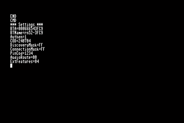
According to http://ww1.microchip.com/downloads/en/devicedoc/50002154a.pdf, GPIO9 needs to be held low for the serial interface to enter command mode. Switching that line high or low will cause the RN52 to report END or CMD. The default serial settings are 115,200 bps, 8N1, with hardware flow-control enabled. GPIO9 is connected to bit 0 of port 1 of U12. The pin is set to output mode by setting $FFD700F to $FE, and then the pin itself set high or low by setting or clearing bit 0 of $FFD700B. Toggling this line in this way does cause the RN52 to report CMD and END appropriately. I can even send the D command to get the current device information, as we can see here:
Now that we can talk to the Bluetooth module, the next step is to find out how to cut its power. Deasserting PWREN does not power the device off. Similarly, cutting the power, but leaving PWREN asserted does not power the device off. However doing both powers it off. This means that the power cut switch alone is not sufficient -- unless the PWREN line is tied to the power enable line for the rail. This change should be made. Plus ideally we should rework the VCC_WIFI_BT power control to actually drop to 0V when the power switch is cut.
ERRATA #8: Connect PWREN of BT module to WiFi/BT power-enable line from IO expander.
Now that we can communicate with the BT module, we can cover off on the smartcard SENSEA line, which is connected to GPIO 12 of the RN52. GPIO12 is normally an input without a pull-up. SENSEA connects to SENSEB when a card is inserted into the smart card reader. Unfortunately we have connected SENSEB to GND, not VCC, so in the default configuration it is not possible to read the smart-card status. However we can switch on a pull-up on GPIO12 using the command I&,3094 to set bit 12 of the pull-up enable register high. This causes SENSEA to go high. Once this has been donte, the I& command can be used to read the GPIO lines. Inserting a card into the smart-card slot causes bit 12 to clear, and with no card inserted, it stays high. Thus we can correctly detect if a smart-card has been inserted.
That completes the first two of the four items for the BT module. Next is general radio function and pairing. As I will need to enter a number of commands, I'll modify the buffered UART test programme to send the various commands to configure the device. This is working fairly well so far. The only challenge I am seeing so far, is that the RN52 seems to only want to be a BT slave, not master. I have vague recollections of reading about different firmware being required for using the RN52 as a master. But if that were the case, I can't find it anywhere now. Also, the version of firmware on the RN52 on the R1 board (1.10) is too old to do firmware upgrade over UART, and only supports upgrade over USB.
I have managed to find the information on using RN52 hardware as a RN52SRC, the master/source version of the module:
https://forum.arduino.cc/index.php?topic=418892.0
And this one that confirms that it can be done, because someone had trouble trying to down-grade back to the RN52 firmware:
https://www.microchip.com/forums/m1027553.aspx
There is also a nice video that someone has made showing the use of an RN52 with the SRC firmware, and pairing with a set of bluetooth speakers:
https://www.youtube.com/watch?v=k_Tfui_o57k
So it looks like, for now, at least, when you turn an RN52 into an RN52SRC, that there is no going back. But I don't want to go in that direction, so its not a problem.
I'll have to make up a bodge USB cable for this, with the D+ and D- directly connected to a chopped USB cable, by the look of things. There is some information on how to do this here:
I don't have easy access to a USB mini connector, so I will try to find a sacrificial USB cable, and just chop the tail off it, and tack it directly onto the D+,D- and GND lines. Here is how I connected it. Quite hacky, but it did the job, allowing the USB connection:

GPIO3 must be asserted on power up, which I can easily arrange, as it is connected to one of the IO expander ports (bit 0 of port 0), so writing $9E to $FFD700F will enable GPIO3 with power on to the RN52, and writing $FE will enable GPIO3 with power off to the RN52.
According to the RN52 documentation, if the RN52 is powered on with GPIO3 held high for 3 seconds, then it should enter Direct Firmware Update (DFU) mode. Presumably at that point it enumerates the USB device as well. But so far, I'm not seeing any USB device show up. I'm also not seeing any indication that the RN52 has entered DFU mode. It is supposed to blink the LED pins (pins 32 and 33) when it enters DFU mode, but that isn't happening, either.
I solved this problem by using the reboot command (R,1) after asserting GPIO3. This then allows a new USB device to be detected:
Bus 001 Device 048: ID 0a12:0001 Cambridge Silicon Radio, Ltd Bluetooth Dongle (HCI mode)
The next step is to use the Microchip firmware update utility, which only works under Windows. Because it needs to do strange USB things, it probably won't work under Wine. But it looks like it might be possible using dfu-util under Linux. The firmware itself can be downloaded from here.
The dfu-util checks the target product ID, which differs between the RN52 and RN52SRC. As a result, I had to build dfu-util from the source, and then comment out the section in src/main.c that checks the product version around line 690. Then I could use this command to replace the firmware:
$ sudo src/dfu-util -d 0a12:ffff,0a12:0001 -D ../rn52src-i_rm100.dfu
dfu-util 0.9
Copyright 2005-2009 Weston Schmidt, Harald Welte and OpenMoko Inc.
Copyright 2010-2016 Tormod Volden and Stefan Schmidt
This program is Free Software and has ABSOLUTELY NO WARRANTY
Please report bugs to http://sourceforge.net/p/dfu-util/tickets/
Deducing device DFU version from functional descriptor length
Opening DFU capable USB device...
ID 0a12:ffff
Run-time device DFU version 0100
Claiming USB DFU Runtime Interface...
Determining device status: state = dfuIDLE, status = 0
dfu-util: WARNING: Runtime device already in DFU state ?!?
Claiming USB DFU Interface...
Setting Alternate Setting #0 ...
Determining device status: state = dfuIDLE, status = 0
dfuIDLE, continuing
DFU mode device DFU version 0100
Device returned transfer size 1023
Copying data from PC to DFU device
Download [=========================] 100% 1071840 bytes
Download done.
dfu-util: unable to read DFU status after completion
To get the RN52 to exit DFU mode I had to completely depower the MEGAphone board: Cutting the power via the IO expander and power switches was insufficient. However, after doing that, I was able to confirm that the firmware has been changed to the RN52SRC 1.00 firmware:

Next step is to confirm that we can see the device in a bluetooth search. This worked with the sink firmware, but the device showed up as a "pager". Now we get this encouraging sign:

But here I have hit a brick wall: It seems that the RN52SRC firmware does not support I2S or SPDIF digital audio -- rather only analog audio. This won't work for the MEGAphone. I have sent a support request to Microchip to see if they have a solution for this. If not, I will need to look at a newer module, like the BM83. There seems to be "audio transceiver" firmware for the BM83, which looks like it might be suitable. But some research will be required.
I have logged case 00566058 with Microchip to see if they can propose a solution. But in the absence of one, I think we might just need to use a different Bluetooth module. Microchip have just got back to me, to say that there is a V1.10 firmware for the RN52SRC that might fix the I2S problem. However, they also indicated that they think we would be better switching to the BM83. If they supply the V1.10 firmware, I will give that a try to get the existing R1 boards working with bluetooth, but I think that switching from the RN52 to the BM83 makes the most sense.
ERRATA #9: Replace RN52 with the BM83.
Microchip have now supplied me with a copy of the V1.10 firmware. As I have already installed the RN52SRC V1.00 firmware, this means that I need to use the UART version of the DFU protocol. The dfu-util above works only over USB. However, https://github.com/quark-mcu/qm-dfu-util may be able to work over UART. To do this, I will need some way to connect the RN52 serial port to my laptop. Possibly the easiest way will be to make a simple bitstream for the FPGA on the MEGAphone board that directly passes through these signals to the serial monitor UART that is available via the JTAG debug adapter.
For the firmware installer, the Visual C++ 2005 Run Time and (on Windows XP) the older Windows XP compatible version (2.08) of the FTDI VCP drivers from here are required. If you try to use the newer FTDI drivers you will get "Code 39" errors. The DFU utility isn't smart enough to switch the module to DFU mode. So you have to use the $ command from the RN52SRC command mode first. It then proceeds without difficulty. All this took me a full and very frustrating day to discover. After all that, it looks like the V1.10 firmware still lacks the I2S commands. So we are back to needing the BM83 instead.
Regardless of the module we use, the current antenna placement is suboptimal, and should be improved.
ERRATA #10: Relocate antenna section to more optional position.
11. LoRa radio
First step is to get the UART communications flowing. It looks like I have the RX and TX lines swapped on these as well. This is just a change to the VHDL pin assignment, which is easy to fix. The LoRa radios ignore hardware flow-control by default, so we don't need to worry about that.
The final preparatory step is to check that the VCC rail to these radios can be switched on and off. This is via port 0, bit 2 of the 3rd IO expander. The power switch is currently changing VCC from ~3.3V to ~2.8V when turned off. So we have a similar problem as with the Bluetooth module being powered through IO lines. The ideal solution to this would be to fully isolate the power domains, by feeding IO lines through opto-isolators.
ERRATA #11: Use opto-isolators to fully segregate devices that can be powered own.
The VCC pin is showing 3.3V now, but the module is currently unresponsive. Probing reveals that the RESET line is tied low. This is strange, given that the schematic indicates that RESET is directly connected to the VCC line. This is the same on both LoRa module pads. As these modules are surface mounted crenelated modules, it isn't possible to cut the trace and tie it to VCC to release the modules from reset with the tools I have here. I have, however tested that the serial lines are now correctly routed. That's as far as I can test without fixing the RESET lines.
ERRATA #12: Correct wiring of /RESET line of LoRa modules.
12. Power switches
The above items have already tested the FPGA, Wifi/Bluetooth and LoRa power switches. The remaining power switches to be tested are those that supply power to the two M.2 communications bays. These switches function. With nothing loaded in those bays, and thus no load on the power railes, the VCC lines decay from 3.3V to 0.4V over several seconds.
15. microSD card slot
This prototype does not automatically boot from the SD card, unlike the previous one. So there is presumably some change that has affected things. The previous prototype had two SD card slots on the same bus, which caused reflections if the one nearere the FPGA was used. Therefore that slot was removed. The pull-up resistors were moved nearer to the FPGA, but the pinout remains unchanged for the SD card slot that remains.
To determine what is going on with this, I will re-activate the SD card bit-bash interface, that will allow me to directly control the lines on the SD card interface. While I wait for that to synthesise, I have confirmed that I can see the clock and MOSI lines, and that they appear to have valid data on them. However, I am not seeing signs of response. VCC_SD should be connected to VCC_FPGA. This is also present.
Comparing
with the working R1 board, all the FPGA pins are correctly connected.
The only difference I see so far, is that one of the pins on the new
board goes low when an SD card is inserted, but which stays high on the
R1 when a card is inserted. This is either the microSD_DAT line or
microSD_CS line. Its ambiguous to me which it is, because the connector
on the FPGA is its own mirror image. I know where microSD clock is, so
from that I can get my point of reference, and determine that it is
microSD_DAT that is going low when an SD card is inserted.
A bit of probing around, reveals that when an SD card is inserted, it is shorting onto some other pin. It's not GND, but I can't see exactly where. It might be time for the microscope again, to see if there are any shorted pads in the SMT. Ah! I have almost certainly found the problem: The microSD/SIM card slot has not located properly when it was reflowed. You can see the problem if you look carefully at the photo below: The top microSD/SIM slot is a little to the left of where the one below it is, and as a result, the pins don't match up properly.

Looking closer, the problem is actually that the entire connector is one pin position to the left of where it should be. This means we have no reason to suspect that the microSD card won't work, were it moved. However, as we have modified the microSD bus, I will feel much more comfortable if I can reflow it into position. I do have a hot air rework station here, so in theory it should be possible to move it.
That said, my soldering station here is outside under a patio, though, and it has been blowing 50km/h wind most of the day, so I may or may not be able to actually do it. It would be less of a worry if I did hot-air reflow on a regular basis, but that's also not the case. I am worried about two things, in particular: (1) That other components will float free and have to be re-seated; and (2) that I will cook the board. A further slightly lesser concern is that the connector might end up with shorted pins when done.
I have made a brief attempt, however I think the number of pins tied to the ground plane renders this job beyond what my little setup here can manage. It really needs more heat in a very targetted way than I can provide here. Perhaps the only thing that might work while I am here would be a set of hot tweezers. So verifying that the microSD card works will have to stand as an errata item.
Errata #13: Test microSD slot after re-seating or on another sample R2 PCB.
This same connector also holds the SIM card for the 2nd M.2 bay, so we will be unable to test the SIM card on that module, without fixing this connector.
14. M.2 bay 1
The M.2 communications bays connect a UART and four PCM audio lines on the bay to the FPGA, as well as several other connections via I2C IO expanders:

The PCM lines are required to be 1.8V logic for the cellular modems. So this is the first thing I will check, to make sure that they are not 3.3V, which could damage the units. Those are fine, and we have VCC 3.3V and GND, so the next lines to check are the RX and TX lines. These are also connected. Whether we have these inverrted, will have to wait until I install a cellular modem to test. Similarly, we can't test the SIM card connector, until then. One issue I have just discovered, is that the UART lines are also supposed to be 1.8V, not 3.3V, with a V_IHMAX of 2.0V. I have previously used one of these modems with 3.3V, but this should still be corrected.
ERRATA #14: Move M.2 UART lines to 1.8V domain.
Before I do put a modem in, I will also check the DTR, W_DISABLE and PERST lines. W_DISABLE is an active-low hardware line to activate Airplane mode. DTR is used to control sleep mode: When low, it activates sleep mode, which minimises power consumption of the modem, while still remaining connected to the cellular network, and able to receive calls, SMS and data. The PERST line is an ouput from the modem in the 1.8V domain that indicates network activity. These lines for the two modems are connected to the third IO expander:
Port 0, bit 7 = DTR, Modem 1 -
Port 1, bit 0 = PERST, Modem 1 - CONFIRMED
Port 1, bit 1 = DTR, Modem 2 - CONFIRMED
Port 1, bit 2 = PERST, Modem 2 - CONFIRMED
Port 1, bit 3 = W_DISABLE, Modem 2 - CONFIRMED
Port 1, bit 4 = W_DISABLE, Modem 1 - CONFIRMED
Knowing that we have the risk of damaging our test modem due to the 3.3V signal voltages, we are ready to test inserting the modem. For this, I need to extract it from the previous prototype.
Module installed in first M.2 bay:


By setting the DTR, PERST and W_DISABLE lines all high, the QC25 4G modem starts up, and can be interacted with via the UART interface, so we know the UART wiring on this bay works fine:

The long stream of @'s is from when the module was de-powered, because the UART_RX line had nothing to pull it high with, and our buffered UART implementation doesn't currently have logic for ignoring this common fault mode for serial ports. Interestingly the UART lines pull-up to 3.3V, so it is possible the documentation about the UART being on the 1.8V domain is incorrect. This should be double-checked.
ERRATA #15: Confirm UART lines voltage domain: 1.8V or 3.3V?
If I have a SIM card inserted, it even detects that, confirmin SIM card communications:

This is helpful, because it will be much easier to test the PCM audio path with a working SIM card. For that, I have just activated a new Telstra SIM card (the only network with coverage around here), so that I can test as I need.
After registering the SIM card, I can send and receive SMS, but not make voice calls. This is most likely because the cell coverage here in the desert is only a Telstra small-site, that supports only VoLTE. The EC25 can apparently do VoLTE according to:
https://www.quectel.com/UploadFile/Product/Quectel_EC25_LTE_Specification_V1.0.pdf
However, some people have had problems doing so:
https://forums.quectel.com/t/ec25-au-brazil-lte-not-sucess-call-over-lte-volte/2575/24
It might be that the 4G module requires a firmware update. This can be done via the 4G network, as I do have a working 4G data connection. Alternatively, the Telstra SIM may not support it, as hinted at here:
http://www.noomio.com.au/wiki/ec21/connecting-ec21-ec25-eg06-or-other-qualcomm-based-platforms/
I can give Telstra a call and ask them what I have to do to enable VoLTE on the SIM card. But more quickly, I can test it with a SIM I have here in my phone that does have VoLTE enabled. That one also only offers the "Generic 3GPP" connection option, and not the "Telstra Commercial VoLTE" one. So I am guessing that it is the EC25 that is the problem. While I have the SIM cards out, I will try the MEGAphone's SIM in my phone, to see if it does VoLTE in that. If so, then I know for sure that the SIM is not the problem as I go forward with the debugging.
While I wait until I get a response from Quectel on how to enable VoLTE on the EC25-AU modem, I can use the audio loopback test functionality of the EC25 to test the PCM audio. This is enabled using the AT+QAUDLOOP=1. We need to first setup the audio format using AT+QDAI=1,0,0,4,0. This should set the module into PCM master mode, the same as has been used on previous tests with earlier MEGAphone prototypes. So if the wiring is right, we should be able to pipe audio to the modem and back again.
With these two commands, I can see the PCM audio clock and SYNC lines coming from the modem. The data in and out are both low, as we are not feeding audio out to the modem from the MEGAphone as yet. In theory once I do, then we should see traffic on both the data out, and the loop-backed data in line.
The PCM_CLK and PCM_SYNC lines get through the voltage converter to the FPGA, and the FPGA responds by supplying sample data. However, that data does not make it through the voltage converter back to the modem. It could be that we have output lines tied together and input lines tied together, and need to swap the PCM_DATA_OUT/IN lines around on the FPGA.
Switching those lines has indeed exstablished an audio loop, which is encouraging. I have also in the meantime received updated firmware from Quectel for the modem. The trick is that it needs a USB interface to flash it, as it is too big an update to use their incremental DFOTA process. This is a bit of a pain, because we don't have USB pins wired to the M.2 connectors, and I don't have an M.2 breakout board handy.
After a lot of digging around, I found direct download links to the Linux software for flashing the modem here: https://core-electronics.com.au/quectel-em05-e-lte-cat-4-m-2-module-seeed-studio.html. With that, and the firmware that Quectel sent me, I was able to update the modem to the latest firmware. That does enable VoLTE, as can be queuried like this:
AT+QMBNCFG="list"
+QMBNCFG: "List",0,0,0,"ROW_Generic_3GPP",0x05010824,201806201
+QMBNCFG: "List",1,0,0,"Reliance_India_VoLTE",0x05011B4B,201801051
+QMBNCFG: "List",2,0,0,"TW_Mobile_China_VoLTE",0x05800301,202005121
+QMBNCFG: "List",3,0,0,"Bouygues_France_VoLTE",0x05800101,202004151
+QMBNCFG: "List",4,0,0,"Telstra-Commercial_VoLTE",0x05800716,202002061
+QMBNCFG: "List",5,0,0,"Commercial-Smartfren",0x05012509,202001041
+QMBNCFG: "List",6,0,0,"VF_Germany_VoLTE",0x05010444,202005121
+QMBNCFG: "List",7,0,0,"TIM_Brasil_VoLTE",0x05800B02,201806061
+QMBNCFG: "List",8,0,0,"VF_Australia_VoLTE",0x05800CE0,202002081
OK
I had to also request that the SIM and service be activated for VoLTE. This required a power cycle of the modem, which I did using the soft power control via the IO expander registers, thus confirming that soft power control of the modem bays functions. Immediately after I was able to make a phone call to the modem from another phone, and PCM audio was visible flowing both ways over the call link, with the network to MEGAphone direction responding to the voice input over the cellular network. The audio flowing in the reverse direction was generated by the MEGAphone, thus confirming PCM audio link.
I have since received feedback from Quectel providing a solution to the out-bound call problem: When dialing, a semi-colon is required after the telephone number. I am not sure if it is required for normal calls, or only VoLTE calls. In any case, it solved the problem. Thus we have confirmed all the connections here.
15. M.2 bay 2
The UART interface has been confirmed working. The PCM interface can be tested using the loop-back mode. However, the SIM card cannot be tested, until the mis-placed SIM card slot on the PCB can be fixed. The PCM audio interface has been checked, and connects to the FPGA pins, and the signals from loop-back mode are available there. However, not audio is seen on the PCM audio data lines. It is possible that these were switched around. These can be switched in the FPGA, so there is no PCB change required.
16. SIM card to M.2 bay connections
As previously mentioned, this cannot be tested until we are able to re-seat the mis-positioned dual microSD/SIM card connector. This will need to be checked on the next spin of the PCB, or when I get some hot tweezers to move the connector.
17. Real-Time Clock
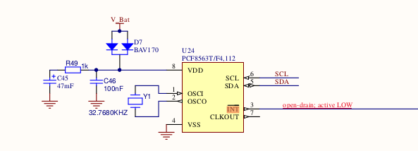
This revision of the MEGAphone uses a PCF8563 Real Time Clock. The MEGA65 has in the meantime switched to an ISL12020MIRZ. For consistency we should use the same RTC chip. That said, the PCB8563 is correctly connected, and can be read using a modified version of the i2cstatus.c programme, and the clock ticks (I have not set the calendar, so the illegal month/year can be ignored):


Errata #16: Switch to ISL12020MIRZ for RTC chip.
18. Accelerometer
The previous images also show the accelerometer values on the fourth line of the display. Between the two images I physically tipped the board, which can be seen in the changed Y value. Thus the accelerometer is working fine.
19. Joystick port
That programme also contains a test for the joystick port, allowing a pointer to be moved around the screen using the joystick. This works correctly.
However, the joystick port currently does not support the POTX/Y lines, which prevents the use of some devices. This will require three FPGA pins
Errata #17: Copy POTX/Y control logic from MEGA65R3.
Nor does it allow the MEGAphone to pull the joystick lines low. This would be desirable, given that the joystick port is a convenient external connection. Ideally for the same reason the joystick lines, or at least one of them, should be promoted to a direct FPGA pin, so that it can be sampled and controlled at high speed. In the simplest form, this could be done by having a single line which can be read rapidly and another line that has a transistor that allows the FPGA to pull the line low, to communicate to an external device. This would require at least two FPGA pins.
Errata #18: Allow high-speed bi-directional communications via joystick port.
The five pins required to improve the joystick port in this way can be obtained by replacing the VGA connector with an HDMI connector. This would leave one free FPGA pin remaining.
The joystick port also protrudes from the rectangular outline of the PCB because, like the VGA connector, it was originally specified as a thinner surface-mount part that proved to be too fragile.
To resolve the protruding joystick connector, this could be moved from its current congested location, to instead be placed immediately below the FPGA module, that is, on the opposite end of the FPGA module to the VGA connector. This would also make it easier to make the high-speed connections described above, as they would not need to be routed across the board. The existing slow IO connections may need to be routed to a nearer IO expander, to make the design routable. Fortunately U12 which is located relatively near by has spare pins.
The components that are currently occupying that space are real-time clock and support components, which are all surface-mount. That circuit already needs to be re-worked, and could be relocated to the area immediate to the right, where there is unused space on the PCB.
Errata #19: Move joystick port from current location to the approximate location of U24, and make the necessary accomodations.
Errata #20: Return the PCB outline to its original rectangular form.
20. headphone jack audio output
The headphone jack output is stereo with two amplifiers, one for each channel. The amplifiers are jointly controlled by bit 7 of the 2nd port of the 3rd IO expander, which is high by default. When I set the audio cross-bar coefficients for the headphone jack to full volume, and ran a game, the music comes out the speaker without problem. Probing with the oscilloscope indicates both amplifiers are working fine.
Plugging in a pair of ear buds, I have confirmed that stereo operation is correct, and I can control the volume of each channel. However, at full volume the volume is REALLY loud, too loud. Also, at quieter volume levels there is quite audible hiss and high-frequency aliasing from the PDM audio output. Looking at the oscilloscope, there is clearly energy at high frequencies, even beyond 1MHz. At modest volume levels, this high-frequency noise swamps the audio signal, and it is is presumably only the attenuation of the speakers that renders the actual audio audible. Thus we need a much better low-pass filter. There are some potential options I have found, including:
https://github.com/MrBuddyCasino/ESP32_MP3_Decoder/blob/master/doc/filter_schematics.png
or even the very simple:
Errata #21: Replace the audio output filter with something that more effectively blocks the high-frequency noise.
Errata #22: Given the very high output volume, consider a solution without audio amplifiers?
21. headphone jack audio input
The audio input is via an AMC1203PSA, which produces a PDM bit stream, similar to that of the MEMS microphones. I have confirmed that the signal arrives at the FPGA connector. However, it is not currently plumbed into the MEGAphone core. I have plumbed it through, and attached it to the last remaining spare input source in the audio mixer, which should allow reading it.
One thing I have noticed is that the headphone jack sense line is not connected. This should be, so that we can implement features like auto-muting the speakers and switching the active mice when a headset is plugged in.
Errata #23: Connect headphone jack sense line to a spare IO expander line.
Returning to the actual audio input, this is not immediately working. I can see a drifting ripple on the processed audio input, but it seems to not be responsive to the headjack microphone.
22. MEMS microphones
The four MEMS microphones were tested using a simple audio visualisation programme that works effectively as an audio-band oscilloscope. This was used to confirm that each of the four microphones were functioning. By tapping on each microphone in turn, it was possible to see the microphone reacting to the transient air pressure, e.g.:

23. Bulk battery connector
To test this, the battery and regulator assembly was removed from the previous prototype and connected, to confirm that the PCB powers up:

The battery and 5V BUC/Boost converter is visible at the top of the image. This is required, because it turns out that a number of components on the MEGAphone require 5V, i.e., the ~3V of the battery is too low. Thus an integrated BUC/BOOST converter is required, or alternatively all components that require >~3V VCC require replacing. It is most likely easier to integrate a BUC/BOOST converter onto the PCB.
Also lacking is a battery charger circuit, ideally one that can charge from solar. It is anticipated that whatever solar panel option we include on the rear of the device will be <2V, and potentially <1V. For example, a single Sunpower high efficiency 125mm x 125mm cell has a maximum power point at ~0.5V. However, it may be possible to get cut solar cell arrangements custom made, e.g., using metsolar.
Errata #24: Include 5V BUC/BOOST converter onto PCB. This may require removing the Smart-Card reader to make space. This is an acceptable trade-off.
Errata #25: Include battery charge circuit.
Errata #26: Include solar regulator circuit, to allow battery charging from a small low-voltage solar.
Errata #27: Include means of measuring the battery voltage, so that battery charge level can be determined.
24. Button inputs
We have a D-PAD, four large buttons and two small rectangular buttons to test.
The D-PAD we already know to be slightly the wrong size as can be seen in the following images:


In short: The spacing between the pads for the switches is currently 18mm, but should be 16mm. The outline hole positions for retaining the light green contact part must also be reduced. The distance between these should be 30mm, rather than the 40mm on the current PCB. The outline of the circle should have a diameter of 29mm, cropped at top and bottom to 27mm.
Errata #28: Fix position and dimensions of D-PAD contacts and markings.
The four buttons on the right hand side now have correctly placed and sized outlines and pads and work reliably:

The two small thin black buttons at the bottom also work. However, these are rather annoying to use, because of their small size. For improved usability, it is better to replace these with two more of the round buttons, which could be fit by moving the buttons a little to the right, or alternatively, we can eliminate the slot in the PCB that was required for the previous version of the touch panel, and leave the buttons in their current position:


Errata #29: Remove smaller of two PCB slots, and replace lower two buttons with the same type as those on the right.
Errata #30: Swap function of the two black buttons and the lower two round buttons, so that power-on and power indicate are where the black buttons were.
25. Thumb-wheel volume inputs
The thumbwheels are connected to the accelerometer's spare ADC inputs.
Here on the R1 board we had a known problem that the voltage divider resistor ladder that was being used to set the voltage range that the thumbwheel potentiometers can produce was wrong, resulting in a very constrained range of values. Experimentation with different values was able to gain general function, however, it was not perfect, and the process of repeatedly switching out small surface-mount resistors to find the correct values was rather tedious. The reason for the resistor ladders not matching the predicted values is most likely due to the tops of R46, R47 and R48 being tied together, thus the total resistance of each circuit affects the voltage at the top of those resistors.
Therefore for the next revision, we should replace the SMT resistor voltage fixed resistors with SMT trim-pots that cover the required range. That is, R46, R47, R48 and R67, R68 and R70 should be all replaced with trimpots. In this way the correct values can be identified, and in the final version the trimpots can be replaced with fixed resistors, if necessary. Or alternatively, the trim pots can remain, which would be helpful for counteracting any variation in the resistance of the thumbwheel potentiometers. This is a possible option for the trimpots. They require ~ 4mm x 6mm of space on the board each, thus an area of ~12x18 mm would be required. This should be possible to find in that area of the board.
To prevent the trimpots being adusted to 0 Ohms and shorting out the VCC_FPGA rail, 1K resistors should be kept in-line with the trim-pots.
Errata #31: Replace R46, R47, R48, R67, R68 and R70 all with 1K resistors, and place 50K Ohm trim-pots serially with each of those resistors.
26. Status indicator LEDs
The status indicator LEDs function, but as previously reported on the R1 PCB, their brightness depends on how hard you press the indicator button. The indicator button should instead be connected to a transistor or similar, so that when pressed, it delivers full current to the LEDs.
Errata #32: Digitise the indicator button input to deliver constant voltage/current to the indicator LEDs.
Also, the indicator LED on the 5V power supply is non-functional. The other indicator LEDs can be illuminated by using a multimeter to probe them. However, that one does not. What is not clear is if the LED is faulty, or if the circuit driving it is problematic. Closer examination reveals that the LED has been inserted backwards. Removing the LED (which destroyed it) and replacing it with another yields an LED that is stuck on.
The LED shows ~5V on one pin, and ~3.3V on the other. This is the LED that is associated with the power supply that is associated with the Q14/Q15 power control circuit that has previously caused problems:


Thus in the least we should change the VCC for the thumbwheels to VCC_MIC, and ideally, more fully investigate this circuit to check its correctness. In particular, the fact that the indicator LED sees ~5V on one pin and ~3.3V on the other pin regardless of whether the indicator line is pulled to ground by the indicator button says that something else is wrong.
Errata #33: Change VCC_FPGA to VCC_MIC on thumbwheels.
Errata #34: Investigate the whole VCC_MIC power rail and associated indicator LED circuit for correctness, as something is clearly wrong with it.
27. All other LEDs
There is one LED that is not a power rail indicaton, which is intended to indicate the status of the virtual disk drive and/or in "secure mode". There is also a high-power IR LED for controlling TVs etc. Neither was plumbed into the VHDL design, and thus were not user-controllable. I have fixed this by connecting them to the floppy LED control line and bit 5 of $D61A, respectively. I have also connected the LED on the TE-0725 FPGA board to bit 4 of $D61A for further debugging support. Even though the LED is not fitted, we can verify that the LED pins are properly controlled by the FPGA.
With this implemented, the floppy LED can now be controlled by the MEGA65 floppy controller. The IR LED can also be controlled, as verified by temporarily fitting a visible light LED to this.
Also, this revision of the PCB does not have an IR receiver. Thus the IR LED can only be used for TV etc remote control purposes. Ideally we would replace it with an IR transceiver, so that MEGAphone devices can communicate using IR light. However, we have a shortage of FPGA pins to achieve this, so it may not be possible. A suitable IR receiver would be a TSP382 series. The TX LED can be modulated at any frequency, so that we can easily cover the 38KHz signal required for most TVs. But we can select a TSP382 that supports the higher 56KHz data rate. If we switch from VGA to an HDMI-style video output, there remains one free FPGA pin, which could be used for this purpose.
28. Soft power on button
This and the following several items are all interrelated, in that using the FPGA power-off pin requires that none of the peripherals that can turn the power back on are attempting to do so.
The soft-power button is treated logically as an interrupt. That is, the soft power on button is one of several sources of interrupt, any of which occurring will cause the FPGA to power on, if it is not disabled by the S7 power-cut switch:

i. The accelerometer, via either of its two active-high interrupt pins.

Alternatively, we can simply disable interrupts from the accelerometer completely. While it is nice, in principle, to be able to trigger the phone to wake up by shaking it or holding it in a particular orientation, or twiddling a thumbwheel, this is a feature that we can easily live without. For testing, we can simply remove Q16 and Q17 to achieve this. Removing it would also make more space for the trim-pots for the thumbwheels.
Errata #36: Fix or remove the accelerometer interrupt circuit.
ii. the I2C IO expanders can also generate interrupts. These are currently all floating high, so not triggering a power on. These could be used to trigger the FPGA to turn on when a given button is pressed (or released), including on the joystick.

These interrupts are fed from pin 1 of each IO expander:

These are all floating high by default, so are not interfering with testing.
iii. Real Time Clock. The RTC interrupt pin is on pin 3, and is also floating high, so not interfering with testing.

Here the problem is the lack of pull-ups on the Ring Indicate lines: If the modem is not installed, but the bay is powered, then the RI line can be interpretted as low by the level converter, resulting in the assertion of the interrupt line.
Errata #37: Add pull-ups to VCC_FPGA on the RI line.
There is a further mystery in that the base of Q2 on modem 1 (but not on modem 2) is at 3.3V, not 0V when the power to the modem bay is turned off, and no modem is installed -- even though all three pins on Q1 are at 0V! Put another way, the base of Q2 is at 3.3V, even though none of the rest of the circuit is at anything other than 0V. That is, there must be an error in the layout of the board, since voltage can't come from nowhere. The same applies to Q2 on modem 2. Is it that the transistors are mis-labeled or is something else weird going on? It is possible that I have just misinterpretted the pinout of the transistors.
Errata #38: Examine and correct layout error on Q2_M1 & Q2_M2.
For actually testing the power control circuit we need a temporary work around to this problem. Probably the easiest option is to remove the Q2_M1 transistor, so that it can't pull the interrupt low. There probably isn't a better way, so I'll do that.
Close examination of the power control circuit reveals that the behaviour of the system is not as expected:

Note that the VCC_FPGA switch, S7, has a different arrangement to the others: Normally pin 1 has the enable line, and pin 3 has GND, so that if the switch is in the 1-2 position, the device is powered, and if in the 2-3 position, then it is off. However for the FPGA, having the switch in the 1-2 position FORCES power to be on, while having it in the 2-3 position places the FPGA power rail under soft control. In this mode, the soft power-on switch and the FPGA power-off line do work. However, the non-indicator LED D2 lights when VCC_FPGA is off.
The polarity of this switch should be reversed to match the others
Errata #39: Swap pins 1 and 3 of S7, so that the "on" position is "on under control of the power control circuit" and "off" is truly off.
This means that the modem and other transistors that I thought were holding the INT line low were in fact fine (as also confirmed by the fact that the FPGA could be switched off using S7).
29. FPGA power off control pin
Working as confirmed in above tests.
30. Real-time clock alarm can power FPGA on
Confirmed. This was tested by enabling a timer interrupt on the RTC chip:
$FFD7026 = $82 = Enable timer, counting at 1Hz
$FFD7027 = $20 = Timer triggers every 32 seconds
$FFD7019 = $01 = Enable timer interrupts.
Then $FFD37fd = $00 to turn of power.
The FPGA then powers off until the timer occurs.
31. M.2 interrupt can power FPGA on
Cannot be tested until the RI lines are reconnected and the necessary pull-up lines installed.
32. One-Time-Pad NOR flash
The NOR flash is intended for storing one-time-pad data, and thus is purposely connected to a slow interface, to prevent an adversary rapidly extracting or replacing the pad material. The trade-off is that it will take a long time for a pair of users to setup their shared pad material.
The connections to the chip are:
SCK - Directly connected to an FPGA pin. This is currently shared with the Smart Card reader. If we replace the smart-card reader with the Raspberry Pi Compute module, we will need to consider if this sharing can continue, or whetehr the NOR flash clock line will need to be moved to an I2C IO expander.
HOLD#/IO3
RESET#
CS2#_NOR
CS1#_NOR
WP#/IO2_NOR
However the SI and SO lines are not currently connected. Without these, communications with this chip is not possible. There are spare lines on the U12 IO expander that could be used to connect these signals: Pin 19 (Port 1, bit 6) could be connected to SI, so that all input lines of the flash memory are connected to the same 8-bit port, so that only one IO write is required to simultaneously set all lines. The only other currently free pin is Pin 9 (Port 0, bit 5), which we have used to connect to the bluetooth power enable line. Assuming that the bluetooth module will be high-impedance on this line, we can make use of that for SO for testing. This will be convenient, since the 0.5mm pitch pins on the IO expander are a pain to accurately solder, but the BT module has nice "big" 1mm pitch pins. So we will in fact connect SI to Pin 6 = GPIO5 on the BT module = Port 0, bit 2 on U12. This will enable me to easily solder up the connections, and start implementing a simple bit-bash interface to talk to the NOR flash. Once we replace the BT module with a BM83, we expect to free up several more pins, and can arrange a more permanent solution.
I attempted to put bodge wires in place for this, but the tools I have here are not quite up to the job, so testing this will have to wait for the next PCB revision, or when I can get some better tools for placing fine bodge wires.
Errata #40: Connect the SI and SO pins of the NOR flash to pins on the U12 IO expander.
The NOR flash is a relatively large IC, which can be fairly easily soldered by hand, due to the 1mm pin spacing. It may be desirable to move it to the opposite side of the PCB, to free-up space, since it can be easily soldered on the reverse side of the PCB. Alternatively there is a BGA version of the part, which would save PCB space.
From a security perspective, there are advantages and disadvantages of both. The construction of the MEGAphone will most likely result in easier access to the component side of the PCB. Thus having either a BGA device with no accessible pins, and/or locating it on the opposite side of the PCB offers some advantages here. However for any such physical protection of access to the pins of the NOR flash, the I2C IO expander to which it is connected must also be protected. It should be possible to locate both the IO expander and NOR flash on the reverse side of the PCB. The IO expander to which it is connected is only otherwise used for GPIO lines to the Bluetooth module (which are likely to be reworked and reduced when switching to the BM83 in any case), one to the smart-card adapter (which is likely to be replaced in favour of a Raspberry Pi Compute Module), and the NOR flash. Thus we can both protect the NOR flash against high-speed access and free up considerable PCB space on the component side. Further protection can be achieved by embedding both the NOR flash and IO expander in epoxy or similar.
Errata #41: Move NOR flash and U12 IO expander to reverse side of PCB.
33. Raspberry Pi Application Processor for running and Android instance.
An anticipated criticism of the MEGAphone will be that it cannot run modern phone apps, e.g., designed for Android. This problem is largely resolveable by allowing the attachment of a slave processor that can run an Android instance. One approach to this is to use a Raspberry Pi Compute Module for this purpose. The latest revision of this board contains 32GB onboard flash, and thus does not require an external SD card. There is also a "lite" version that does use an external SD card slot. As we have an unused SD card slot on the 2nd SIM card/SDcard slot, it probably makes sense to use the "lite" version.
The compute module itself is 68mm x 30mm compared with the 60mm x 40mm footprint of the Smart card. There are vertical and horizontal connectors.
The vertical connector ~78mm wide -- almost 20mm wider than the smart-card connector. This would require considerable rearrangement of the PCB. A vertical connector would also considerably increase the thickness of the MEGAphone, which is already going to be rather thick. This this is less attractive.
The horizontal connector is ~72mm wide, which would be much easier to accommodate. As has been done with the M.2 bays, it should be possible to put some components under the Pi Compute Module to regain some of the space. As this is not possible with the smart-card connector, this represents a probably net gain of PCB space. This is important, because adding a Pi Compute Module will also require some additional components.
In particular, to allow the sharing of the panel display, a set of bus multiplexors will be required to connect and disconnect the Pi from the panel bus. The easiest approach would have the Pi be the master of the panel bus when connected. The MEGAphone's MEGA65 core supports GenLock, so it would be possible to switch the HSYNC, VSYNC and DE lines on the FPGA to inputs, and follow the display of the Pi Compute Module, and then take selectively take control of the bus on a pixel-by-pixel basis, allowing the MEGAphone to display overlays over the Pi Display for various purposes, e.g., to indicate incoming calls, that would still be managed in the more secure domain of the MEGAphone.
A challenge for this, is that with all the other changes, there are no free FPGA pins: The two pins freed up by removing the Smart Card would be consumed by the UART interface to communicate with the Pi Compute Module. The deficit is one pin for the display bus control. In the worst case, that could be controlled via an I2C IO expander, but then the timing precision will be greatly reduce. This would still be sufficient to allow an upper third or lower third type approach, but not a with pixel-by-pixel resolution. This means the upper/lower thirds would have to be in landscape orientation, because the panel scans along its long axis.
Account will also have to be taken for any increased height that the Pi Compute Module protrudes above the height of other components that must sit under the battery. Also, the heat dissipation of the Pi Compute Module may become an issue. The overall energy efficiency of the Pi Computer Module is a matter of residual concern. The large battery of the MEGAphone should, however, still be able to run the Pi Compute Module for several hours under a normal work-load.
A further goal would be to have two additional FPGA pins that connect to the Pi Compute module, so that transparent emulation of the touch screen can be provided to the Pi. This will also make it possible to implement transparent accessibility support for standard Android builds running on the Pi Compute Module, supporting one of the alternative use-cases of the MEGAphone. That said, it may be possible with very minor changes to the Android build to provide synthetic touch panel status via the UART communications interface.
Errata #42: Explore the feasibility of switching the smart-card connector for a Raspberry Pi Compute Module and associated interface circuitry.
Errata #43: Explore the options for providing synthetic touch panel events to the Android instance running on the Pi Compute Module.
99.Miscellaneous
It actually took a bit of fiddling around
to get this far, as one of the transistors that powers the back light,
Q15, was the wrong type, and we had to implement a work-around by
putting a different transistor on, and adding a bodge-wire. This was preventing the microphones from getting their 5V power rail.


However, it is not clear if the bodge wire on the MEGAphone R2 PCB is the result of having initially installed the wrong component, or whether there remains a fault that was solved by the bodge implemented on the PCB. Unfortunately the memory of which reflects reality has been lost. This will need to be reinvestigated on the next PCB that gets assembled. A student is currently assembling a MEGAphone R2 PCB for their project, which will hopefully allow this question to be answered.
Errata #44: Confirm the correct circuit arrangement required for Q15.
Summary
As expected, there are a number of known and discovered problems with the R2 PCB. However it looks like all of these should be solvable, and it should be possible to also make several significant improvments, like being able to host a Raspberry Pi Compute Module to make it possible to run Android apps on the MEGAphone in a sandboxed environment. It should be possible to reduce the PCB size back to the original size, and achieve all this without losing any important functionality -- only the SD card reader will need to go, and that was of only limited use at best for most use-cases.
In terms of the milestone, we have covered all of the required steps, and actually gone some way towards completing the 3rd milestone, which focuses on developing the revised bill of materials and modified placement of components.
Strewth Paul, you been busy!
ReplyDeleteThat was a great read.
Thanks, and glad you enjoyed it!
DeleteMost of what was written above flies over my head. :D
ReplyDeleteWith that being said, the Phone-version of the Mega65 is what I am looking forward to the most, and I have felt it has been far to 'quiet on the internet' about this since that amazing video came out: https://www.youtube.com/watch?v=KuNB4ocZDXA
So to see so much progress for the Phone is marvelous! Splendid!