This one is a super simple one: It just has the 3.5mm audio jack on it. It's a bit questionable as to whether this even needs to be on a module, vs just be soldered directly onto the carrier board. But I still like the idea of it being on a module to allow easier re-use, as I iterate the main board. Also, it's about the size project that I can tackle on my lunch break.
1. Key Component Selection
The only component it needs is the connector itself.
We need to support stereo audio plus microphone input, and nothing else. So probably something like one of these should be okay:
https://www.digikey.com.au/en/products/detail/same-sky-formerly-cui-devices/SJ-43515RS-SMT-TR/669722
Trying to find the symbols and footprints for KiCad for this connector, I was a bit surprised that it's not even listed in SnapEDA.com -- but the datasheet actually has links to the files from the vendor directly! It would be nice if all vendors included such links in their datasheets. It just removes that bit of friction for selecting a component, and isn't that hard to do.
Anyway, with that in place, and knowing that I need only 4 pins, it's time to think about the module layout -- in particular that this connector needs to sit on the edge of the board, which the standard castellated modules I have created don't handle explicitly. That said, the only real chance is the module bay footprint, to remove the furniture at one end of the module.
Meanwhile, I have been annoyed by a problem that I'd encountered before, but forgotten the solution for: KiCad freezes for several seconds when switching between the schematic and PCB windows. It turns out its a known problem with running KiCad under XWayland, and the solution is to make sure no KiCad window is maximised. The interested reader can go down the rabbit hole to understand why this happens, but I'm just glad I remembered I'd seen the problem before, and could easily deal with it, because it's really annoying, and a big productivity and mood drag.
2. Schematic Layout
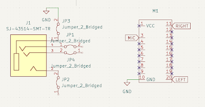
Okay, for the schematic, this is super simple: We have 4 pins that need to go to 4 pads on the module. Nothing else. The only other thing I've added is cuttable jumpers for each of the four pins, in case I get the pin order wrong (again).
3. PCB Layout
The PCB layout itself is also super simple. The main thing is to try to keep the size of the module as small as possible. Once I know the dimensions of the active area of the module, I can create a castellated module footprint that will fit it:
Okay, so now we know the size we need. Note that unlike most of the other modules, for this one, the jack has to sit on the flat size of the module, rather than the side that will sit in the cut-out on rear-side. This means that the module can actually be a whisker smaller than it would otherwise be. So let's set this up.
Okay, so a 2x10 is a fair bit longer than we need. 2x7 should be enough, so it's probably worth making that size module, rather than wasting ~7.5mm at the tail-end.
In the process, I have also updated all of the other footprints to fix the castellation hole sizes, and some other minor things that I was having to fix in each derived footprint, so that it should be quicker to make new footprints in future. I do also wonder if I can't come up with a way to parametrically generate the footprints, as it should be quite possible given KiCad's text format for footprints. I'll have a think about it.
But in the meantime, here is what the module looks like now:
And that's really all there is to this one.


No comments:
Post a Comment